|
|
|
PDF MAX1133 Data sheet ( Hoja de datos )
| Número de pieza | MAX1133 | |
| Descripción | 16-Bit ADC / 200ksps / 5V Single-Supply with Reference | |
| Fabricantes | Maxim Integrated | |
| Logotipo | ||
Hay una vista previa y un enlace de descarga de MAX1133 (archivo pdf) en la parte inferior de esta página. Total 19 Páginas | ||
|
No Preview Available !
19-2083; Rev 0; 8/01
16-Bit ADC, 200ksps, 5V Single-Supply
with Reference
General Description
The MAX1132/MAX1133 are 200ksps, 16-bit ADCs.
These serially interfaced ADCs connect directly to
SPI™, QSPI™, and MICROWIRE™ devices without
external logic. They combine an input scaling network,
internal track/hold, clock, a +4.096V reference, and
three general-purpose digital output pins (for external
multiplexer or PGA control) in a 20-pin SSOP package.
The excellent dynamic performance (SINAD ≥ 85dB),
high-speed (200ksps), and low power (7.5mA) of these
ADCs, make them ideal for applications such as indus-
trial process control, instrumentation, and medical
applications. The MAX1132 accepts input signals of 0
to +12V (unipolar) or ±12V (bipolar), while the
MAX1133 accepts input signals of 0 to +4.096V (unipo-
lar) or ±4.096V (bipolar). Operating from a single
+4.75V to +5.25V analog supply and a +4.75V to
+5.25V digital supply, power-down modes reduce
current consumption to 1mA at 10ksps and further
reduce supply current to less than 20µA at slower data
rates. A serial strobe output (SSTRB) allows direct con-
nection to the TMS320 family of digital signal proces-
sors. The MAX1132/MAX1133 user can select either the
internal clock, or an external serial-interface clock for
the ADC to perform analog-to-digital conversions.
The MAX1132/MAX1133 feature internal calibration cir-
cuitry to correct linearity and offset errors. On-demand
calibration allows the user to optimize performance.
Three user-programmable logic outputs are provided
for the control of an 8-channel mux or a PGA.
Applications
Industrial Process Control
Industrial I/O Modules
Data-Acquisition Systems
Medical Instruments
Portable and Battery-Powered Equipment
Functional Diagram appears at end of data sheet.
Typical Application Circuit appears at end of data sheet.
SPI and QSPI are trademarks of Motorola, Inc.
MICROWIRE is a trademark of National Semiconductor Corp.
Features
o 200ksps (Bipolar) and 150ksps (Unipolar)
Sampling ADC
o 16-Bits, No Missing Codes
o 1.5LSB INL Guaranteed
o 85dB (min) SINAD
o +5V Single-Supply Operation
o Low-Power Operation, 7.5mA (Unipolar Mode)
o 2.5µA Shutdown Mode
o Software-Configurable Unipolar and Bipolar Input
Ranges
0 to +12V and ±12V (MAX1132)
0 to +4.096V and ±4.096V (MAX1133)
Internal or External Reference
o Internal or External Clock
o SPI/QSPI/MICROWIRE-Compatible Serial Interface
o Three User-Programmable Logic Outputs
o Small 20-Pin SSOP Package
Ordering Information
PART
MAX1132ACAP*
MAX1132BCAP
TEMP. RANGE PIN-PACKAGE
0°C to +70°C 20 SSOP
0°C to +70°C 20 SSOP
INL
(LSB)
±1.5
±2.5
Ordering Information continued at end of data sheet.
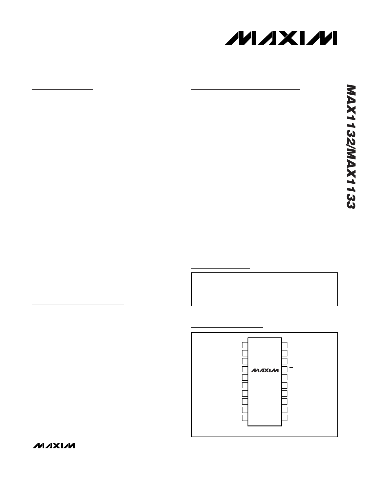
Pin Configuration
TOP VIEW
REF 1
REFADJ 2
AGND 3
AVDD 4
DGND 5
SHDN 6
P2 7
P1 8
P0 9
SSTRB 10
MAX1132
MAX1133
20 AIN
19 AGND
18 CREF
17 CS
16 DIN
15 DVDD
14 DGND
13 SCLK
12 RST
11 DOUT
SSOP
________________________________________________________________ Maxim Integrated Products 1
For pricing, delivery, and ordering information, please contact Maxim/Dallas Direct! at
1-888-629-4642, or visit Maxim’s website at www.maxim-ic.com.
1 page 
16-Bit ADC, 200ksps, 5V Single-Supply
with Reference
TIMING CHARACTERISTICS (Figures 5 and 6)
(AVDD = DVDD = +5V ±5%, TA = TMIN to TMAX, unless otherwise noted.)
PARAMETER
Acquisition Time
DIN to SCLK Setup
DIN to SCLK Hold
SCLK to DOUT Valid
CS Fall to DOUT Enable
CS Rise to DOUT Disable
CS to SCLK Rise Setup
CS to SCLK Rise Hold
SCLK High Pulse Width
SCLK Low Pulse Width
SCLK Fall to SSTRB
CS Fall to SSTRB Enable
CS Rise to SSTRB Disable
SSTRB Rise to SCLK Rise
RST Pulse Width
SYMBOL
tACQ
tDS
tDH
tDO
tDV
tTR
tCSS
tCSH
tCH
tCL
tSSTRB
tSDV
tSTR
tSCK
tRS
CONDITIONS
CLOAD = 50pF
CLOAD = 50pF
CLOAD = 50pF
CLOAD = 50pF, external clock mode
CLOAD = 50pF, external clock mode
Internal clock mode
MIN TYP MAX UNITS
1.14 µs
50 ns
0 ns
70 ns
80 ns
80 ns
100 ns
0 ns
80 ns
80 ns
80 ns
80 ns
80 ns
0 ns
208 ns
Note 1: Tested at AVDD = DVDD = +5V, bipolar input mode.
Note 2: Relative accuracy is the deviation of the analog value at any code from its theoretical value after the gain error and offset
error have been nulled.
Note 3: Offset nulled.
Note 4: Conversion time is defined as the number of clock cycles multiplied by the clock period, clock has 50% duty cycle.
Includes the acquisition time.
Note 5: ADC performance is limited by the converter’s noise floor, typically 300µVp-p.
Note 6: When an external reference has a different voltage than the specified typical value, the full scale of the ADC will scale
proportionally.
Note 7: Electrical characteristics are guaranteed from AVDD(MIN) = DVDD(MIN) to AVDD(MAX) = DVDD(MAX). For operations beyond
this range, see the Typical Operating Characteristics. For guaranteed specifications beyond the limits, contact the factory.
Note 8: Defined as the change in positive full scale caused by a ±5% variation in the nominal supply voltage.
_______________________________________________________________________________________ 5
5 Page 
16-Bit ADC, 200ksps, 5V Single-Supply
with Reference
CS
SCLK
DIN
SSTRB
tACQ
14
8
START
UNI/
BIP
INT/
EXT
M1
M0
P2
P1
P0
DOUT
A/D
STATE
IDLE
ACQUISITION
15 19 29 32
B15
MSB
B14
B13
B4
B3
B2
B1
B0
LSB
FILLED WITH
ZEROS
CONVERSION
IDLE
Figure 3. Long Acquisition Mode (32-Clock Cycles) External Clock, Bipolar Mode
low for a maximum of 6µs, during which time SCLK
should remain low for best noise performance. An inter-
nal register stores data when the conversion is in
progress. SCLK clocks the data out of the internal stor-
age register at any time after the conversion is com-
plete.
The MSB of the conversion is available at DOUT when
SSTRB goes high. The subsequent 15 falling edges on
SCLK shift the remaining bits out of the internal storage
register (Figure 4). CS does not need to be held low
once a conversion is started.
When internal clock mode is selected, SSTRB does not
go into a high-impedance state when CS goes high.
Figure 5 shows the SSTRB timing in internal clock
mode. In internal clock mode, data can be shifted in to
the MAX1132/MAX1133 at clock rates up to 4.8MHz,
provided that the minimum acquisition time, tACQ, is
kept above 1.14µs in bipolar mode and 1.82µs in
unipolar mode. Data can be clocked out at 8MHz.
Output Data
The output data format is straight binary for unipolar
conversions and two’s complement in bipolar mode. In
both modes the MSB is shifted out of the MAX1132/
MAX1133 first.
Data Framing
The falling edge of CS does NOT start a conversion on
the MAX1132/MAX1133. The first logic high clocked into
DIN is interpreted as a start bit and defines the first bit of
the Control Byte. A conversion starts on the falling edge
of SCLK, after the seventh bit of the Control Byte (the P1
bit) is clocked into DIN. The start bit is defined as:
The first high bit clocked into DIN with CS low any-
time the converter is idle, e.g., after AVDD is
applied, or as the first high bit clocked into DIN
after CS is pulsed high, then low.
OR
If a falling edge on CS forces a start bit before the
conversion or calibration is complete, then the
current operation will be terminated and a new
one started.
Applications Information
Power-On Reset
When power is first applied to the MAX1132/MAX1133
or if RST is pulsed low, the internal calibration registers
are set to their default values. The user-programmable
registers (P0, P1, and P2) are low, and the device is
configured for bipolar mode with internal clocking.
Calibration
To compensate the MAX1132/MAX1133 for temperature
drift and other variations, they should be periodically
calibrated. After any change in ambient temperature
more than 10°C the device should be recalibrated. A
100mV change in supply voltage or any change in the
reference voltage should be followed by a calibration.
Calibration corrects for errors in gain, offset, integral
nonlinearity, and differential nonlinearity. The MAX1132/
MAX1133 should be calibrated after power-up or the
assertion of reset. Make sure the power supplies and
the reference voltage have fully settled prior to initiating
the calibration sequence.
Initiate calibration by setting M1 = 0 and M0 = 1 in the
Control-Byte. In internal clock mode, SSTRB goes low at
______________________________________________________________________________________ 11
11 Page | ||
| Páginas | Total 19 Páginas | |
| PDF Descargar | [ Datasheet MAX1133.PDF ] | |
Hoja de datos destacado
| Número de pieza | Descripción | Fabricantes |
| MAX113 | +3V / 400ksps / 4/8-Channel / 8-Bit ADCs with 1UA Power-Down | Maxim Integrated |
| MAX11300 | 20-Port Programmable Mixed-Signal I/O | Maxim Integrated |
| MAX11301 | 20-Port Programmable Mixed-Signal I/O | Maxim Integrated |
| MAX11311 | 12-Port Programmable Mixed-Signal I/O | Maxim Integrated |
| Número de pieza | Descripción | Fabricantes |
| SLA6805M | High Voltage 3 phase Motor Driver IC. |
Sanken |
| SDC1742 | 12- and 14-Bit Hybrid Synchro / Resolver-to-Digital Converters. |
Analog Devices |
|
DataSheet.es es una pagina web que funciona como un repositorio de manuales o hoja de datos de muchos de los productos más populares, |
| DataSheet.es | 2020 | Privacy Policy | Contacto | Buscar |