|
|
PDF SDA9205-2 Data sheet ( Hoja de datos )
| Número de pieza | SDA9205-2 | |
| Descripción | Triple 8-Bit Analog-to-Digital-Converter | |
| Fabricantes | Siemens | |
| Logotipo |  |
|
Hay una vista previa y un enlace de descarga de SDA9205-2 (archivo pdf) en la parte inferior de esta página. Total 30 Páginas | ||
|
No Preview Available !
Triple 8-Bit Analog-to-Digital-Converter
SDA 9205-2
Preliminary Data
Features
q Three equivalent CMOS A/D converters on chip
q 30-MHz sample rate
q 8-bit resolution
q No external sample & hold required
q On-chip input buffer for each analog channel
q Internal clamping circuits for each of the ADCs
q Different digital output multiplex formats:
– 3 independent unmultiplexed 8-bit outputs
– Multiplexed formats compatible to inputs of all
Siemens Featureboxes and Siemens TV-SAM
– CCIR 656 output format
q Overflow and underflow outputs
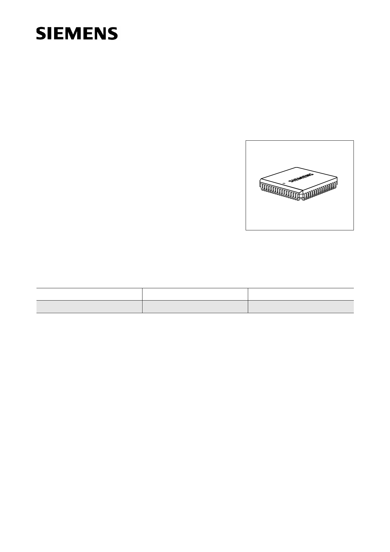
CMOS IC
P-LCC-68-1
Type
SDA 9205-2
Ordering Code
Q67100-H5069
Package
P-LCC-68-1 (SMD)
General Description
The SDA 9205-2 is a single monolithic IC containing three separate 8-bit analog to digital converters
for video (YUV) applications. It utilizes an advanced VLSI 1.2 µm CMOS process providing 30-MHz
sampling rates at 8 bits. Different digital output multiplex formats are selectable on chip via several
control inputs, compatible to inputs of all Siemens Featureboxes, Siemens TV-SAM, and CCIR 656
output format.
The ADCs have no missing codes over the full operating temperature range of 0 to + 70 °C.
Operation is from + 5 V DC-power supply.
Semiconductor Group
1
01.94
1 page 
SDA 9205-2
Circuit Description
Analog to Digital Converter
The SDA 9205-2 implements 3 independent 8-bit analog-to-digital converters.
They are two step converters with a coarse comparator block and two fine comparator blocks each
using pipeline architecture for high speed sampling performance. During the first clock cycle, the
coarse comparator samples and determines 4 MSBs and one of the fine comparator blocks
samples the input voltage. During the second clock cycle this fine comparator block makes its
decision for the 4 LSBs. So the coarse comparator block makes its decisions at each clock cycle,
the fine comparator blocks make the comparison alternating every two clock cycles.
The converter uses the redundancy principle to correct fine conversion. The sample and hold
function has been distributed in each comparator due to the two step conversion principle.
Clamping
An internal clamping circuit is provided in each of three analog channels. The analog pins AINA,
AINB, AINC are switched simultaneously to on chip generated clamping levels by an active high
pulse on pin 30 (CLAMP).
Clamping Levels
Analog Channel
AINA
AINB, AINC
Dual Code
00010000
10000000
Components
(Y)
(U, V)
Semiconductor Group
5
5 Page 
SDA 9205-2
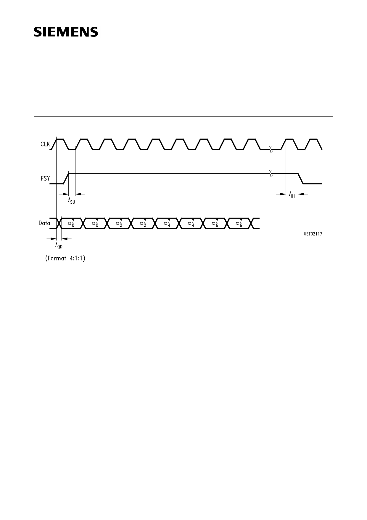
The digital output data are synchronized by the FSY signal. The first high of FSY defines the first
output format byte and is synchronized to CLK. In case of asynchronism the first (in formats 8:1:1,
4:1:1 the first and the second) output format byte after FSY had gone high does not contain valid
data. Timing of FSY, CLK and output data is shown in figure 4 with output format 4:1:1.
Figure 4
Semiconductor Group
11
11 Page | ||
| Páginas | Total 30 Páginas | |
| PDF Descargar | [ Datasheet SDA9205-2.PDF ] | |
Hoja de datos destacado
| Número de pieza | Descripción | Fabricantes |
| SDA9205-2 | Triple 8-Bit Analog-to-Digital-Converter | Siemens |
| Número de pieza | Descripción | Fabricantes |
| SLA6805M | High Voltage 3 phase Motor Driver IC. |
Sanken |
| SDC1742 | 12- and 14-Bit Hybrid Synchro / Resolver-to-Digital Converters. |
Analog Devices |
|
DataSheet.es es una pagina web que funciona como un repositorio de manuales o hoja de datos de muchos de los productos más populares, |
| DataSheet.es | 2020 | Privacy Policy | Contacto | Buscar |
