|
|
|
PDF 74VCX16838 Data sheet ( Hoja de datos )
| Número de pieza | 74VCX16838 | |
| Descripción | Low Voltage 16-Bit Selectable Register/Buffer with 3.6V Tolerant Inputs and Outputs | |
| Fabricantes | Fairchild Semiconductor | |
| Logotipo | ||
Hay una vista previa y un enlace de descarga de 74VCX16838 (archivo pdf) en la parte inferior de esta página. Total 7 Páginas | ||
|
No Preview Available !
www.DataSheet4U.com
July 1997
Revised July 2000
74VCX16838
Low Voltage 16-Bit Selectable Register/Buffer
with 3.6V Tolerant Inputs and Outputs
General Description
The VCX16838 contains sixteen non-inverting selectable
buffered or registered paths. The device can be configured
to operate in a registered, or flow through buffer mode by
utilizing the register enable (REGE) and Clock (CP) sig-
nals. The device operates in a 16-bit word wide mode. All
outputs can be placed into 3-State through use of the OE
Pin. These devices are ideally suited for buffered or regis-
tered 168 pin and 200 pin SDRAM DIMM memory mod-
ules.
The 74VCX16838 is designed for low voltage (1.65V to
3.6V) VCC applications with I/O compatibility up to 3.6V.
The 74VCX16838 is fabricated with an advanced CMOS
technology to achieve high speed operation while maintain-
ing low CMOS power dissipation.
Features
s Compatible with PC100 and PC133 DIMM module
specifications
s 1.65V–3.6V VCC supply operation
s 3.6V tolerant inputs and outputs
s tPD (CP to On)
3.0 ns max for 3.0V to 3.6V VCC
4.0 ns max for 2.3V to 2.7V VCC
8.0 ns max for 1.65V to 1.95V VCC
s Power-off high impedance inputs and outputs
s Supports live insertion and withdrawal (Note 1)
s Static Drive (IOH/IOL)
±24 mA @ 3.0V VCC
±18 mA @ 2.3V VCC
±6 mA @ 1.65V VCC
s Uses patented noise/EMI reduction circuitry
s Ideal for SDRAM DIMM modules
s Latch-up performance exceeds 300 mA
s ESD performance:
Human body model > 2000V
Machine model > 200V
Note 1: To ensure the high-impedance state during power up or power
down, OE should be tied to VCC through a pull-up resistor; the minimum
value of the resistor is determined by the current-sourcing capability of the
driver.
Ordering Code:
Order Number Package Number
Package Description
74VCX16838MTD
MTD48
48-Lead Thin Shrink Small Outline Package (TSSOP), JEDEC MO-153, 6.1mm Wide
Devices also available in Tape and Reel. Specify by appending suffix letter “X” to the ordering code.
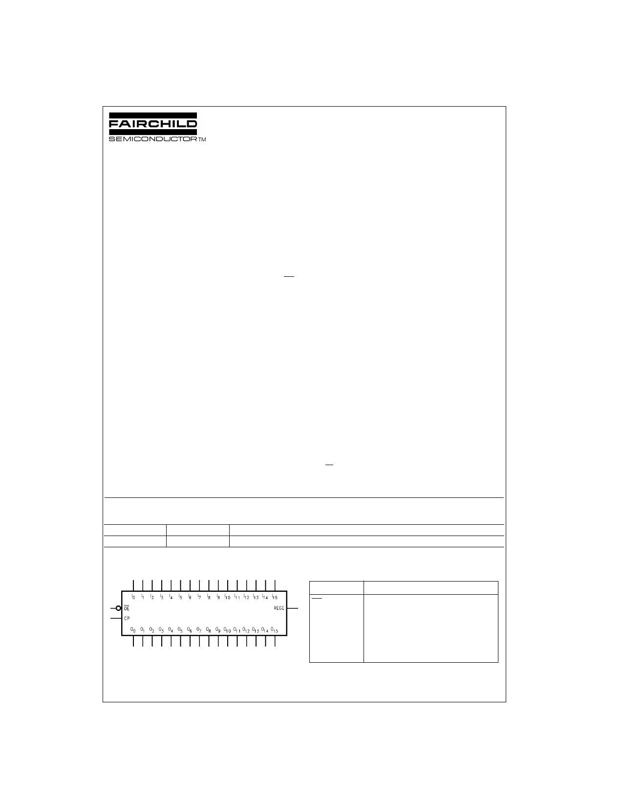
Logic Symbol
Pin Descriptions
Pin Names
OE
I0–I15
O0–O15
CP
REGE
Description
Output Enable Input (Active LOW)
Inputs
Outputs
Clock Pulse Input
Register Enable Input
© 2000 Fairchild Semiconductor Corporation DS500034
www.fairchildsemi.com
1 page 
AC Electrical Characteristics (Note 8)
TA = −40°C to +85°C, CL = 30 pF, RL = 500Ω
Symbol
Parameter
VCC = 3.3V ± 0.3V
VCC = 2.5V ± 0.2V
VCC = 1.8V ± 0.15V
Units
Min Max Min Max Min Max
fMAX
tPHL, tPLH
Maximum Clock Frequency
Prop Delay In to On
(REGE = 0)
250 200 100 MHz
0.8 2.5 1.0 3.5 1.5 7.0 ns
tPHL, tPLH Prop Delay CP to On
(REGE = 1)
0.8 3.0 1.0 4.0 1.5 8.0 ns
tPHL, tPLH Prop Delay REGE to On
0.8 3.0 1.0 4.0 1.5 8.0 ns
tPZL, tPZH Output Enable Time
0.8 3.5 1.0 4.7 1.5 9.4 ns
tPLZ, tPHZ Output Disable Time
0.8 3.5 1.0 3.9 1.5 7.0 ns
tS Setup Time
1.0 1.0 2.5
ns
tH Hold Time
0.7 0.7 1.0
ns
tW Pulse Width
1.5 1.5 4.0
ns
tOSHL
tOSLH
Output to Output Skew
(Note 9)
0.5 0.5 0.75 ns
Note 8: For CL = 50PF, add approximately 300 ps to the AC maximum specification.
Note 9: Skew is defined as the absolute value of the difference between the actual propagation delay for any two separate outputs of the same device. The
specification applies to any outputs switching in the same direction, either HIGH-to-LOW (tOSHL) or LOW-to-HIGH (tOSLH).
Extended AC Electrical Characteristics (Note 10)
Symbol Parameter
tPHL, tPLH Prop Delay In to On (REGE = 0)
tPHL, tPLH Prop Delay CP to On (REGE = 1)
tPHL, tPLH Prop Delay REGE to On
tPZL, tPZH Output Enable Time
tPLZ, tPHZ Output Disable Time
tS Setup Time
tH Hold Time
Note 10: This parameter is guaranteed by characterization but not tested.
TA = −0°C to +85°C, RL = 500Ω VCC = 3.3V ± 0.3V
CL = 50 pF
Min Max
1.0 2.8
1.4 3.3
1.0 3.3
1.0 3.8
1.0 3.8
1.0
0.7
Units
ns
ns
ns
ns
ns
ns
ns
Dynamic Switching Characteristics
Symbol
Parameter
VOLP
Quiet Output Dynamic Peak VOL
VOLV
Quiet Output Dynamic Valley VOL
VOHV
Quiet Output Dynamic Valley VOH
Conditions
CL = 30 pF, VIH = VCC, VIL = 0V
CL = 30 pF, VIH = VCC, VIL = 0V
CL = 30 pF, VIH = VCC, VIL = 0V
VCC
(V)
TA = +25°C
Typical
Units
1.8 0.25
2.5 0.6
V
3.3 0.8
1.8 −0.25
2.5 −0.6
V
3.3 −0.8
1.8 1.5
2.5 1.9
V
3.3 2.2
Capacitance
Symbol
Parameter
CIN
COUT
CPD
Input Capacitance
Output Capacitance
Power Dissipation Capacitance
Conditions
VCC = 1.8V, 2.5V or 3.3V, VI = 0V or VCC
VI = 0V or VCC, VCC = 1.8V, 2.5V or 3.3V
VI = 0V or VCC, f = 10 MHz,
VCC = 1.8V, 2.5V or 3.3V
TA = +25°C
Typical
6
7
20
Units
pF
pF
pF
5 www.fairchildsemi.com
5 Page | ||
| Páginas | Total 7 Páginas | |
| PDF Descargar | [ Datasheet 74VCX16838.PDF ] | |
Hoja de datos destacado
| Número de pieza | Descripción | Fabricantes |
| 74VCX16835 | Low Voltage 18-Bit Universal Bus Driver with 3.6V Tolerant Inputs and Outputs | Fairchild Semiconductor |
| 74VCX16838 | Low Voltage 16-Bit Selectable Register/Buffer with 3.6V Tolerant Inputs and Outputs | Fairchild Semiconductor |
| 74VCX16839 | Low Voltage 20-Bit Selectable Register/Buffer with 3.6V Tolerant Inputs and Outputs | Fairchild Semiconductor |
| Número de pieza | Descripción | Fabricantes |
| SLA6805M | High Voltage 3 phase Motor Driver IC. |
Sanken |
| SDC1742 | 12- and 14-Bit Hybrid Synchro / Resolver-to-Digital Converters. |
Analog Devices |
|
DataSheet.es es una pagina web que funciona como un repositorio de manuales o hoja de datos de muchos de los productos más populares, |
| DataSheet.es | 2020 | Privacy Policy | Contacto | Buscar |