|
|
|
PDF 74LVX594 Data sheet ( Hoja de datos )
| Número de pieza | 74LVX594 | |
| Descripción | LOW VOLTAGE CMOS 8 BIT SHIFT REGISTER WITH OUTPUT REGISTER (5V TOLERANT INPUTS) | |
| Fabricantes | STMicroelectronics | |
| Logotipo | ||
Hay una vista previa y un enlace de descarga de 74LVX594 (archivo pdf) en la parte inferior de esta página. Total 14 Páginas | ||
|
No Preview Available !
74LVX594
LOW VOLTAGE CMOS 8 BIT SHIFT REGISTER
WITH OUTPUT REGISTER (5V TOLERANT INPUTS)
s HIGH SPEED:
tPD = 5.5ns (TYP.) at VCC = 3.3V
s 5V TOLERANT INPUTS
s INPUT VOLTAGE LEVEL:
VIL=0.8V, VIH=2V at VCC=3V
s LOW POWER DISSIPATION:
ICC = 4 µA (MAX.) at TA=25°C
s LOW NOISE:
VOLP = 0.3V (TYP.) at VCC = 3.3V
s SYMMETRICAL OUTPUT IMPEDANCE:
|IOH| = IOL = 4mA (MIN)
s BALANCED PROPAGATION DELAYS:
tPLH ≅ tPHL
s OPERATING VOLTAGE RANGE:
VCC(OPR) = 2V to 3.6V (1.2V Data Retention)
s PIN AND FUNCTION COMPATIBLE WITH
74 SERIES 594
s IMPROVED LATCH-UP IMMUNITY
s POWER DOWN PROTECTION ON INPUTS
DESCRIPTION
The 74LVX594 is a low voltage CMOS 8 BIT
SHIFT REGISTER WITH OUTPUT REGISTER
fabricated with sub-micron silicon gate and
double-layer metal wiring C2MOS technology. It is
ideal for low power, battery operated and low
noise 3.3V applications.
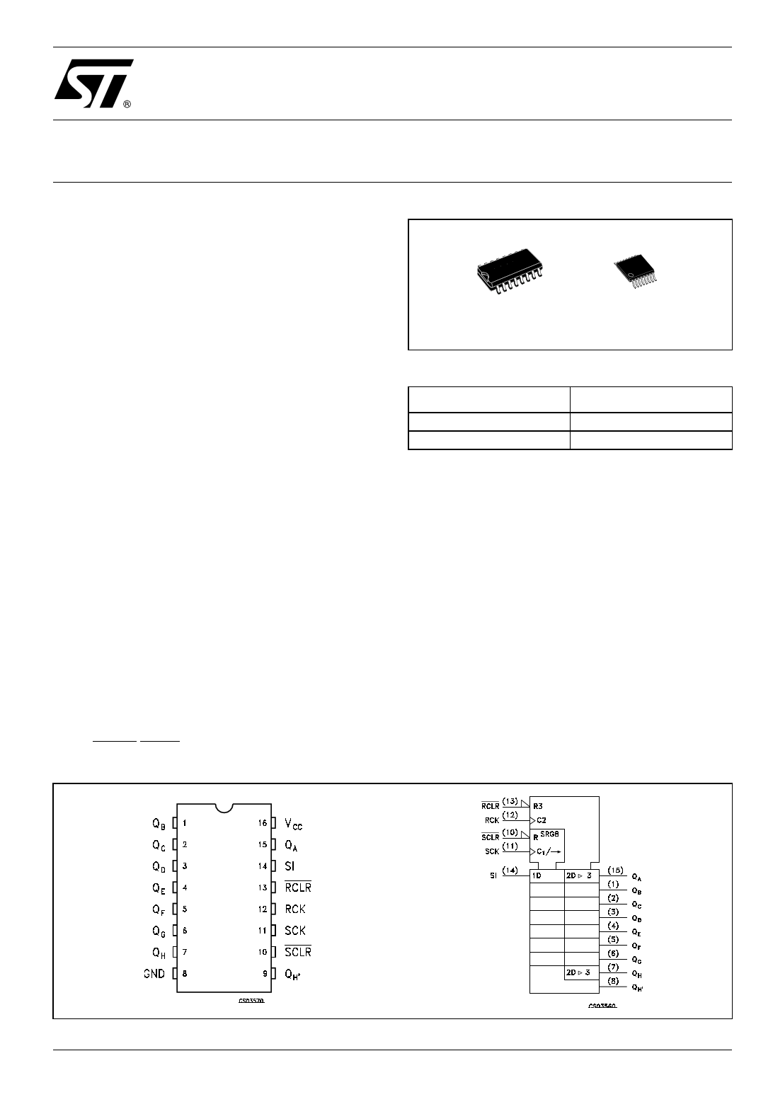
This device contains an 8-bit serial-in, parallel-out
shift register that feeds an 8-bit D-type storage
register. Separate clocks and direct overriding
clear (SCLR, RCLR) are provided for both the shift
SOP
TSSOP
Table 1: Order Codes
PACKAGE
SOP
TSSOP
T&R
74LVX594MTR
74LVX594TTR
register and the storage register. A serial (QH’)
output is provided for cascading purposes. Both
the shift register and storage register use
positive-edge triggered clocks. If the clocks are
connected together, the shift register state will
always be one clock pulse ahead of the storage
register.
Power down protection is provided on all inputs
and 0 to 7V can be accepted on inputs with no
regard to the supply voltage. This device can be
used to interface 5V to 3V system. It combines
high speed performance with the true CMOS low
power consumption.
All inputs and outputs are equipped with
protection circuits against static discharge, giving
them 2KV ESD immunity and transient excess
voltage.
Figure 1: Pin Connection And IEC Logic Symbols
August 2004
Rev. 5
1/14
1 page 
74LVX594
Table 5: Recommended Operating Conditions
Symbol
VCC
VI
VO
Top
dt/dv
Parameter
Supply Voltage (note 1)
Input Voltage
Output Voltage
Operating Temperature
Input Rise and Fall Time (note 2) (VCC = 3.3V)
1) Truth Table guaranteed: 1.2V to 3.6V
2) VIN from 0.8V to 2.0V
Table 6: DC Specifications
Value
2 to 3.6
0 to 5.5
0 to VCC
-55 to 125
0 to 100
Unit
V
V
V
°C
ns/V
Test Condition
Value
Symbol
Parameter
VCC
(V)
VIH High Level Input
Voltage
VIL Low Level Input
Voltage
VOH High Level Output
Voltage
2.0
3.0
3.6
2.0
3.0
3.6
2.0
3.0
3.0
VOL Low Level Output
Voltage
2.0
3.0
3.0
II Input Leakage
Current
3.6
Ioff
Power Off Leakage
Current
0
ICC
Quiescent Supply
Current
3.6
IO=-50 µA
IO=-50 µA
IO=-4 mA
IO=50 µA
IO=50 µA
IO=4 mA
VI = 5V or GND
VI = 0 to 5V
VI = VCC or GND
TA = 25°C
-40 to 85°C -55 to 125°C Unit
Min.
1.5
2.0
2.4
1.9
2.9
2.58
Typ.
2.0
3.0
0.0
0.0
Max.
0.5
0.8
0.8
0.1
0.1
0.36
Min.
1.5
2.0
2.4
1.9
2.9
2.48
Max.
0.5
0.8
0.8
0.1
0.1
0.44
Min.
1.5
2.0
2.4
1.9
2.9
2.4
Max.
0.5
0.8
0.8
0.1
0.1
0.55
V
V
V
V
± 0.1
±1
± 1 µA
± 0.1
±5
± 5 µA
4 40 40 µA
Table 7: Dynamic Switching Characteristics
Test Condition
Value
Symbol
Parameter
VOLP
VOLV
VIHD
VILD
Dynamic Low Voltage
Quiet Output (note 1, 2)
Dynamic High Voltage
Input (note 1, 3)
Dynamic Low Voltage
Input (note 1, 3)
VCC
TA = 25°C
-40 to 85°C -55 to 125°C Unit
(V) Min. Typ. Max. Min. Max. Min. Max.
0.3 0.5
3.3
-0.5 -0.3
3.3 CL = 50 pF 2
V
3.3 0.8
1) Worst case package.
2) Max number of outputs defined as (n). Data inputs are driven 0V to 3.3V, (n-1) outputs switching and one output at GND.
3) Max number of data inputs (n) switching. (n-1) switching 0V to 3.3V. Inputs under test switching: 3.3V to threshold (VILD), 0V to threshold
(VIHD), f=1MHz.
5/14
5 Page 
DIM.
A
C
D
N
T
Ao
Bo
Ko
Po
P
74LVX594
Tape & Reel SO-16 MECHANICAL DATA
MIN.
12.8
20.2
60
6.45
10.3
2.1
3.9
7.9
mm.
TYP
MAX.
330
13.2
22.4
6.65
10.5
2.3
4.1
8.1
MIN.
0.504
0.795
2.362
0.254
0.406
0.082
0.153
0.311
inch
TYP.
MAX.
12.992
0.519
0.882
0.262
0.414
0.090
0.161
0.319
11/14
11 Page | ||
| Páginas | Total 14 Páginas | |
| PDF Descargar | [ Datasheet 74LVX594.PDF ] | |
Hoja de datos destacado
| Número de pieza | Descripción | Fabricantes |
| 74LVX594 | LOW VOLTAGE CMOS 8 BIT SHIFT REGISTER WITH OUTPUT REGISTER (5V TOLERANT INPUTS) | STMicroelectronics |
| 74LVX594MTR | LOW VOLTAGE CMOS 8 BIT SHIFT REGISTER WITH OUTPUT REGISTER (5V TOLERANT INPUTS) | STMicroelectronics |
| 74LVX594TTR | LOW VOLTAGE CMOS 8 BIT SHIFT REGISTER WITH OUTPUT REGISTER (5V TOLERANT INPUTS) | STMicroelectronics |
| Número de pieza | Descripción | Fabricantes |
| SLA6805M | High Voltage 3 phase Motor Driver IC. |
Sanken |
| SDC1742 | 12- and 14-Bit Hybrid Synchro / Resolver-to-Digital Converters. |
Analog Devices |
|
DataSheet.es es una pagina web que funciona como un repositorio de manuales o hoja de datos de muchos de los productos más populares, |
| DataSheet.es | 2020 | Privacy Policy | Contacto | Buscar |