|
|
|
PDF MAX104 Data sheet ( Hoja de datos )
| Número de pieza | MAX104 | |
| Descripción | 5V / 1Gsps / 8-Bit ADC with On-Chip 2.2GHz Track/Hold Amplifier | |
| Fabricantes | Maxim Integrated | |
| Logotipo | ||
Hay una vista previa y un enlace de descarga de MAX104 (archivo pdf) en la parte inferior de esta página. Total 30 Páginas | ||
|
No Preview Available !
19-1459; Rev 1; 5/99
EVAALVUAAILTAIOBNLEKIT
±5V, 1Gsps, 8-Bit ADC with
On-Chip 2.2GHz Track/Hold Amplifier
General Description
The MAX104 PECL-compatible, 1Gsps, 8-bit analog-to-
digital converter (ADC) allows accurate digitizing of
analog signals with bandwidths to 2.2GHz. Fabricated
on Maxim’s proprietary advanced GST-2 bipolar
process, the MAX104 integrates a high-performance
track/hold (T/H) amplifier and a quantizer on a single
monolithic die.
The innovative design of the internal T/H, which has an
exceptionally wide 2.2GHz full-power input bandwidth,
results in high performance (greater than 7.5 effective
bits) at the Nyquist frequency. A fully differential com-
parator design and decoding circuitry reduce out-of-
sequence code errors (thermometer bubbles or sparkle
codes) and provide excellent metastable performance
of one error per 1016 clock cycles. Unlike other ADCs
that can have errors resulting in false full- or zero-scale
outputs, the MAX104 limits the error magnitude to
1LSB.
The analog input is designed for either differential or
single-ended use with a ±250mV input voltage range.
Dual, differential, PECL-compatible output data paths
ensure easy interfacing and include an 8:16 demulti-
plexer feature that reduces output data rates to one-half
the sampling clock rate. The PECL outputs can be
operated from any supply between +3V to +5V for com-
patibility with +3.3V or +5V referenced systems. Control
inputs are provided for interleaving additional MAX104
devices to increase the effective system sampling rate.
The MAX104 is packaged in a 25mm x 25mm, 192-con-
tact Enhanced Super-Ball Grid Array (ESBGA™) and is
specified over the commercial (0°C to +70°C) tempera-
ture range.
Applications
Digital RF/IF Signal Processing
Direct RF Downconversion
High-Speed Data Acquisition
Digital Oscilloscopes
High-Energy Physics
Radar/Sonar/ECM Systems
ATE Systems
Features
o 1Gsps Conversion Rate
o 2.2GHz Full-Power Analog Input Bandwidth
o >7.5 Effective Bits at fIN = 500MHz (Nyquist
Frequency)
o ±0.25LSB INL and DNL
o 50Ω Differential Analog Inputs
o ±250mV Input Signal Range
o On-Chip, +2.5V Precision Bandgap Voltage
Reference
o Latched, Differential PECL Digital Outputs
o Low Error Rate: 10-16 Metastable States at 1Gsps
o Selectable 8:16 Demultiplexer
o Internal Demux Reset Input with Reset Output
o 192-Contact ESBGA Package
Ordering Information
PART
MAX104CHC
TEMP. RANGE
0°C to +70°C
PIN-PACKAGE
192 ESBGA
192-Contact ESBGA
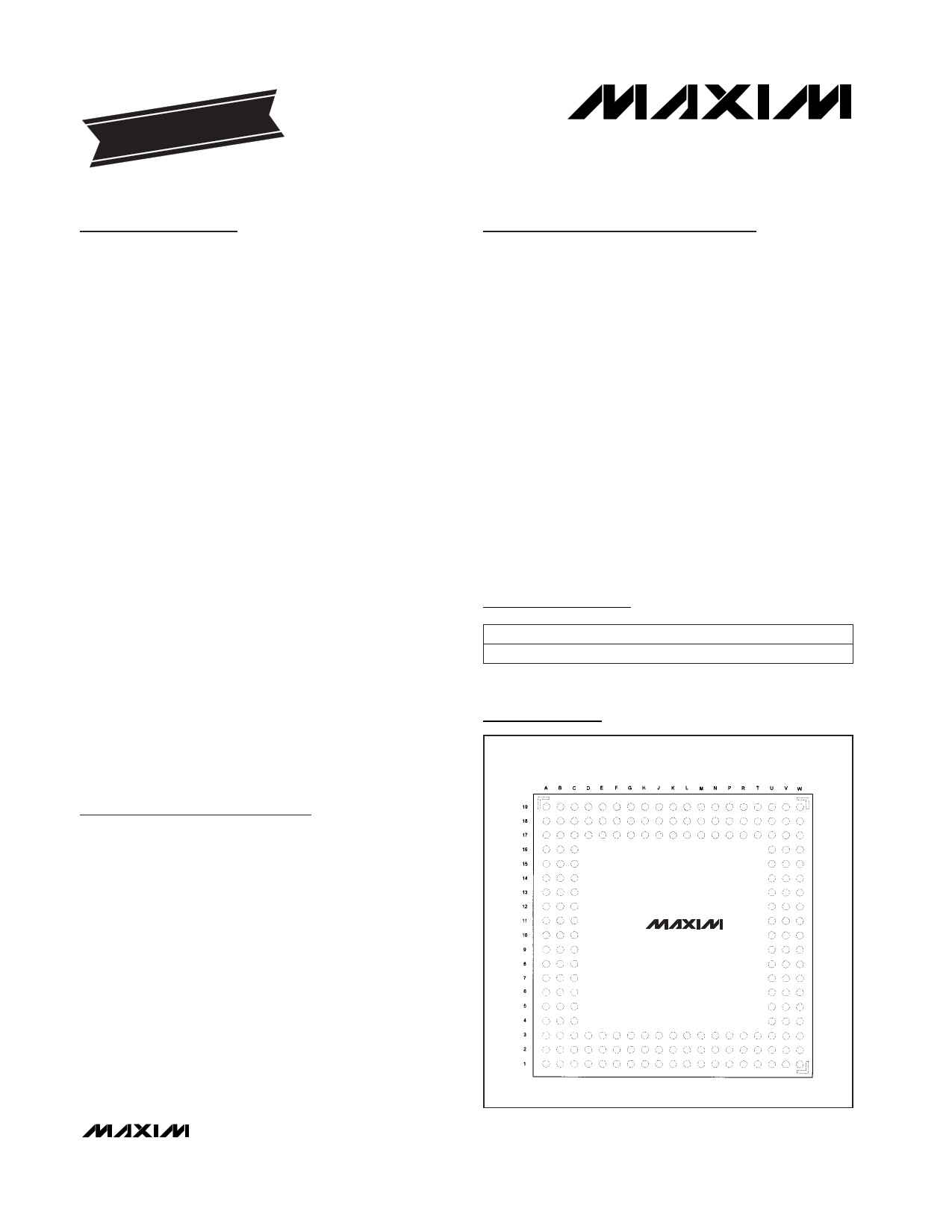
Ball Assignment Matrix
TOP VIEW
MAX104
Typical Operating Circuit appears at end of data sheet.
ESBGA is a trademark of Amkor/Anam.
ESBGA
________________________________________________________________ Maxim Integrated Products 1
For the latest literature: http://www.maxim-ic.com, or phone 1-800-998-8800.
For small orders, phone 1-800-835-8769.
1 page 
±5V, 1Gsps, 8-Bit ADC with
On-Chip 2.2GHz Track/Hold Amplifier
AC ELECTRICAL CHARACTERISTICS (continued)
(VCCA = VCCI = VCCD = +5.0V, VEE = -5.0V, VCCO = +3.3V, REFIN connected to REFOUT, fS = 1Gsps, fIN at -1dBFS, TA = +25°C,
unless otherwise noted.)
PARAMETER
TIMING CHARACTERISTICS
Maximum Sample Rate
Clock Pulse Width Low
Clock Pulse Width High
Aperture Delay
Aperture Jitter
Reset Input Data Setup Time
(Note 13)
SYMBOL
fMAX
tPWL
tPWH
tAD
tAJ
tSU
Figure 17
Figure 17
Figure 4
Figure 4
Figure 15
CONDITIONS
MIN TYP MAX UNITS
1
0.45
0.45
100
<0.5
0
Gsps
ns
5 ns
ps
ps
ps
Reset Input Data Hold Time
(Note 13)
tHD Figure 15
0 ps
CLK to DREADY Propagation
Delay
tPD1 Figure 17
2.2 ns
DREADY to DATA Propagation
Delay (Note 14)
tPD2 Figure 17
-50 150 350 ps
DATA Rise Time
DATA Fall Time
DREADY Rise Time
DREADY Fall Time
Primary Port Pipeline
Delay
Auxiliary Port Pipeline
Delay
tRDATA
tFDATA
tRDREADY
tFDREADY
tPDP
tPDA
20% to 80%, CL = 3pF
20% to 80%, CL = 3pF
20% to 80%, CL = 3pF
20% to 80%, CL = 3pF
Figures 6, 7, 8
DIV1, DIV2 modes
DIV4 mode
Figures 6, 7, 8
DIV1, DIV2 modes
DIV4 mode
420 ps
360 ps
220 ps
180 ps
7.5 Clock
7.5 Cycles
8.5 Clock
9.5 Cycles
Note 1: Static linearity parameters are computed from a “best-fit” straight line through the code transition points. The full-scale
range (FSR) is defined as 256 · slope of the line.
Note 2: The offset control input is a self-biased voltage divider from the internal +2.5V reference voltage. The nominal open-circuit
voltage is +1.25V. It may be driven from an external potentiometer connected between REFOUT and GNDI.
Note 3: The clock input’s termination voltage can be operated between -2.0V and GNDI. Observe the absolute maximum ratings
on the CLK+ and CLK- inputs.
Note 4: Input logic levels are measured with respect to the VCCO power-supply voltage.
Note 5: All PECL digital outputs are loaded with 50Ω to VCCO - 2.0V. Measurements are made with respect to the VCCO power-
supply voltage.
Note 6: The current in the VCCO power supply does not include the current in the digital output’s emitter followers, which is a func-
tion of the load resistance and the VTT termination voltage.
Note 7: Common-Mode Rejection Ratio is defined as the ratio of the change in the transfer-curve offset voltage to the change in
the common-mode voltage, expressed in dB.
Note 8: Power-Supply Rejection Ratio is defined as the ratio of the change in the transfer-curve offset voltage to the change in
power-supply voltage, expressed in dB.
Note 9: Measured with the positive supplies tied to the same potential; VCCA = VCCD = VCCI. VCC varies from +4.75V to +5.25V.
Note 10: VEE varies from -5.25V to -4.75V.
_______________________________________________________________________________________ 5
5 Page 
±5V, 1Gsps, 8-Bit ADC with
On-Chip 2.2GHz Track/Hold Amplifier
CONTACT
J1
J17
J18
K17
K18
L1
L17
L18
M17
M18
N17
N18
P1
P2
P17
P18
R1, R2, R3
R19
T1
U10
U11
U12
U13
U14
U15
U16
V10
V11
V12
V13
V14
V15
V16
Pin Description (continued)
NAME
VIN-
A3-
A3+
DREADY-
DREADY+
VIN+
P4-
P4+
A4-
A4+
P5-
P5+
CLK-
TESTPOINT (T.P.)
A5-
A5+
CLKCOM
AUXEN1
CLK+
RSTIN-
RSTOUT-
OR-
A7-
P7-
A6-
P6-
RSTIN+
RSTOUT+
OR+
A7+
P7+
A6+
P6+
FUNCTION
Differential Input Voltage (-)
Complementary Auxiliary Output Data Bit 3
Auxiliary Output Data Bit 3
Complementary Data-Ready Clock
Data-Ready Clock
Differential Input Voltage (+)
Complementary Primary Output Data Bit 4
Primary Output Data Bit 4
Complementary Auxiliary Output Data Bit 4
Auxiliary Output Data Bit 4
Complementary Primary Output Data Bit 5
Primary Output Data Bit 5
Complementary Sampling-Clock Input
This contact must be connected to GNDI.
Complementary Auxiliary Output Data Bit 5
Auxiliary Output Data Bit 5
50Ω Clock Termination Return
Tie to VCCO to power the auxiliary port. Tie to GNDD to power
down.
Sampling Clock Input
Complementary PECL Demux Reset Input
Complementary PECL Reset Output
Complementary PECL Overrange Bit
Complementary Auxiliary Output Data Bit 7 (MSB)
Complementary Primary Output Data Bit 7 (MSB)
Complementary Auxiliary Output Data Bit 6
Complementary Primary Output Data Bit 6
PECL Demux Reset Input
PECL Reset Output
PECL Overrange Bit
Auxiliary Output Data Bit 7 (MSB)
Primary Output Data Bit 7 (MSB)
Auxiliary Output Data Bit 6
Primary Output Data Bit 6
______________________________________________________________________________________ 11
11 Page | ||
| Páginas | Total 30 Páginas | |
| PDF Descargar | [ Datasheet MAX104.PDF ] | |
Hoja de datos destacado
| Número de pieza | Descripción | Fabricantes |
| MAX100 | 250Msps / 8-Bit ADC with Track/Hold | Maxim Integrated |
| MAX1002 | Low-Power / 60Msps / Dual / 6-Bit ADC | Maxim Integrated |
| MAX1003 | Low-Power / 90Msps / Dual 6-Bit ADC | Maxim Integrated |
| MAX1005 | IF Undersampler | Maxim Integrated |
| Número de pieza | Descripción | Fabricantes |
| SLA6805M | High Voltage 3 phase Motor Driver IC. |
Sanken |
| SDC1742 | 12- and 14-Bit Hybrid Synchro / Resolver-to-Digital Converters. |
Analog Devices |
|
DataSheet.es es una pagina web que funciona como un repositorio de manuales o hoja de datos de muchos de los productos más populares, |
| DataSheet.es | 2020 | Privacy Policy | Contacto | Buscar |