|
|
|
PDF IDT54FCT825AT Data sheet ( Hoja de datos )
| Número de pieza | IDT54FCT825AT | |
| Descripción | HIGH-PERFORMANCE CMOS BUS INTERFACE REGISTERS | |
| Fabricantes | Integrated Device | |
| Logotipo | ||
Hay una vista previa y un enlace de descarga de IDT54FCT825AT (archivo pdf) en la parte inferior de esta página. Total 9 Páginas | ||
|
No Preview Available !
IDT54/74FCT821AT/BT/CT, 823/825AT/BT/CT/DT
HIGH-PERFORMANCE CMOS BUS INTERFACE REGISTERS
MILITARY AND COMMERCIAL TEMPERATURE RANGES
HIGH-PERFORMANCE
IDT54/74FCT821AT/BT/CT
CMOS BUS
INTERFACE REGISTERS
IDT54/74FCT823AT/BT/CT/DT
IDT54/74FCT825AT/BT/CT
Integrated Device Technology, Inc.
FEATURES:
• Common features:
– Low input and output leakage ≤1µA (max.)
– CMOS power levels
– True TTL input and output compatibility
– VOH = 3.3V (typ.)
– VOL = 0.3V (typ.)
– Meets or exceeds JEDEC standard 18 specifications
– Product available in Radiation Tolerant and Radiation
Enhanced versions
– Military product compliant to MIL-STD-883, Class B
and DESC listed (dual marked)
– Available in DIP, SOIC, SSOP, QSOP, CERPACK
and LCC packages
• Features for FCT821T/FCT823T/FCT825T:
– A, B, C and D speed grades
– High drive outputs (-15mA IOH, 48mA IOL)
– Power off disable outputs permit “live insertion”
DESCRIPTION:
The FCT82xT series is built using an advanced dual metal
CMOS technology. The FCT82xT series bus interface regis-
ters are designed to eliminate the extra packages required to
buffer existing registers and provide extra data width for wider
address/data paths or buses carrying parity. The FCT821T
are buffered, 10-bit wide versions of the popular FCT374T
function. The FCT823T are 9-bit wide buffered registers with
Clock Enable (EN) and Clear (CLR) – ideal for parity bus
interfacing in high-performance microprogrammed systems.
The FCT825T are 8-bit buffered registers with all the FCT823T
controls plus multiple enables (OE1, OE2, OE3) to allow multi-
user control of the interface, e.g., CS, DMA and RD/WR. They
are ideal for use as an output port requiring high IOL/IOH.
The FCT82xT high-performance interface family can drive
large capacitive loads, while providing low-capacitance bus
loading at both inputs and outputs. All inputs have clamp
diodes and all outputs are designed for low-capacitance bus
loading in high-impedance state.
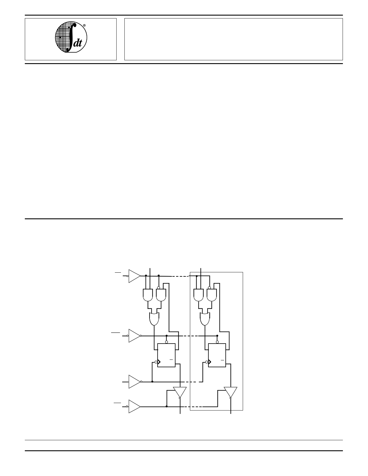
FUNCTIONAL BLOCK DIAGRAM
D0
EN
DN
CLR
CP
D CL Q
CP Q
D CL Q
CP Q
OE
Y0
The IDT logo is a registered trademark of Integrated Device Technology, Inc.
MILITARY AND COMMERCIAL TEMPERATURE RANGES
©1995 Integrated Device Technology, Inc
66..2211
YN
2567 drw 01
AUGUST 1995
DSC-42102/5
1
1 page 
IDT54/74FCT821AT/BT/CT, 823/825AT/BT/CT/DT
HIGH-PERFORMANCE CMOS BUS INTERFACE REGISTERS
MILITARY AND COMMERCIAL TEMPERATURE RANGES
POWER SUPPLY CHARACTERISTICS
Symbol
Parameter
Test Conditions(1)
Min. Typ.(2) Max. Unit
∆ICC
ICCD
Quiescent Power Supply Current
TTL Inputs HIGH
Dynamic Power Supply Current(4)
VCC = Max.
VIN = 3.4V(3)
VCC = Max.
VIN = VCC
— 0.5 2.0 mA
— 0.15 0.25 mA/
Outputs Open
VIN = GND
MHz
OE = EN = GND
One Input Toggling
50% Duty Cycle
IC
Total Power Supply Current(6)
VCC = Max.
VIN = VCC
— 1.5 3.5 mA
Outputs Open
VIN = GND
fCP= 10MHz
50% Duty Cycle
OE = EN = GND
One Bit Toggling
VIN = 3.4V
VIN = GND
— 2.0 5.5
at fi = 5MHz
50% Duty Cycle
VCC = Max.
VIN = VCC
— 3.8 7.3(5)
Outputs Open
VIN = GND
fCP= 10MHz
50% Duty Cycle
OE = EN = GND
Eight Bits Toggling
VIN = 3.4V
VIN = GND
— 6.0 16.3(5)
at fi = 2.5MHz
50% Duty Cycle
NOTES:
1. For conditions shown as Max. or Min., use appropriate value specified under Electrical Characteristics for the applicable device type.
2. Typical values are at VCC = 5.0V, +25°C ambient.
3. Per TTL driven input (VIN = 3.4V). All other inputs at VCC or GND.
4. This parameter is not directly testable, but is derived for use in Total Power Supply Calculations.
5. Values for these conditions are examples of the ICC formula. These limits are guaranteed but not tested.
6. IC = IQUIESCENT + IINPUTS + IDYNAMIC
IC = ICC + ∆ICC DHNT + ICCD (fCP/2 + fiNi)
ICC = Quiescent Current
∆ICC = Power Supply Current for a TTL High Input (VIN = 3.4V)
DH = Duty Cycle for TTL Inputs High
NT = Number of TTL Inputs at DH
ICCD = Dynamic Current Caused by an Input Transition Pair (HLH or LHL)
fCP = Clock Frequency for Register Devices (Zero for Non-Register Devices)
fi = Input Frequency
Ni = Number of Inputs at fi
All currents are in milliamps and all frequencies are in megahertz.
2567 tbl 07
6.21 5
5 Page | ||
| Páginas | Total 9 Páginas | |
| PDF Descargar | [ Datasheet IDT54FCT825AT.PDF ] | |
Hoja de datos destacado
| Número de pieza | Descripción | Fabricantes |
| IDT54FCT825A | HIGH-PERFORMANCE CMOS BUS INTERFACE REGISTERS | Integrated Device |
| IDT54FCT825AT | HIGH-PERFORMANCE CMOS BUS INTERFACE REGISTERS | Integrated Device |
| Número de pieza | Descripción | Fabricantes |
| SLA6805M | High Voltage 3 phase Motor Driver IC. |
Sanken |
| SDC1742 | 12- and 14-Bit Hybrid Synchro / Resolver-to-Digital Converters. |
Analog Devices |
|
DataSheet.es es una pagina web que funciona como un repositorio de manuales o hoja de datos de muchos de los productos más populares, |
| DataSheet.es | 2020 | Privacy Policy | Contacto | Buscar |