|
|
PDF M64898GP Data sheet ( Hoja de datos )
| Número de pieza | M64898GP | |
| Descripción | PLL FREQUENCY SYNTHESIZER WITH DC-DC CONVERTER FOR PC | |
| Fabricantes | Mitsubishi | |
| Logotipo |  |
|
Hay una vista previa y un enlace de descarga de M64898GP (archivo pdf) en la parte inferior de esta página. Total 8 Páginas | ||
|
No Preview Available !
MITSUBISHI ICs (TV)
M64898GP
PLL FREQUENCY SYNTHESIZER WITH DC-DC CONVERTER FOR PC
DESCRIPTION
The M64898GP is a semiconductor integrated circuit consisting of
PLL frequency synthesizer for TV/VCR /PC.
It contains the prescaler with operating up to1.3GHz,4 band drivers
and DC-DC converter for Tuning voltage.
FEATURES
• Built-in DC-DC converter for Tuning voltage
• 4 integrated PNP band drivers
(Io=30mA, Vsat=0.2V typ@VCC1 to 10V )
• Built-in prescaler with input amplifier (max=1.3GHz)
• PLL lock/unlock status display out put
(Built-in pull up resistor)
• X’tal 4MHz is used to realize 3 type of tuning steps
(Divider ratio 1/512, 1/640, 1/1024)
• Software compatible with M64892/M64893
• Automatick switching of tuning step according to the
number of data bits (62.5kHz at 18bits , 32.25kHz at 19bits)
• Built-in Power on reset system
• Small Package(SSOP)
APPLICATION
PC, TV, VCR tuners
PIN CONFIGURATION (TOP VIEW)
PRESCALER
INPUT
GND
SUPPLY
VOLTAGE 1
SUPPLY
VOLTAGE 2
fin
GND
VCC1
VCC2
BS4
1
2
3
4
5
BAND
SWITCHING
OUTPUTS
BS3 6
BS2 7
BS1
DC-DCSUPPLY
VOLTAGE
VDC
PEACK CURRENT
DETECT
lpk
8
9
10
20 Xin
19 ENA
CRYSTAL
OSCILLATOR
ENABLE INPUT
18 DATA DATA INPUT
17 CLK CLOCK INPUT
16
LD/ftest
LD/ftest
OUTPUT
15
CONT
fREF
SWITCHING
14 Vin FILTER INPUT
13 Vtu
12 +B
11 SWE
TUNING
OUTPUT
SUPPLY
VOLTAGE
SWITCHING
OUTPUT
Outline 20P2E-A
RECOMMENDED OPERATING CONDITION
Supply voltage range..............................................VCC1=4.5 to 5.5V
VCC2=VCC1 to 10V
Rated supply voltage...........................................................VCC1=5V
VCC2=VCC1
BLOCK DIAGRAM
VCC1
3
Xin 20
OSC
f REF DIVIDER
fin 1
AMP
1/8
CNT
15
SELECTER
LATCH
2
LATCH
15
DIV.
VDC
9
SQ
R
-
+ Vreg
CLK 17
DATA 18
ENA 19
1/32,1/33
15bit
PROGRAMMABLE DIVIDER
18/19-bit SHIFT REGISTER
CONTROL
PHASE
DETECTOR
LOCK
DETECTOR
5
CHARGE
PUMP
CP TEST
LATCH
BAIS / BAND SWITCH DRIVER
4567
VCC2
BS4
BS3
BS2
8
BS1
4
Power
On Reset
2
GND
lpk
10
11 SWE
12 +B
13 Vtu
OS
14 Vin
16 LD/ftest
1
1 page 
MITSUBISHI ICs (TV)
M64898GP
PLL FREQUENCY SYNTHESIZER WITH DC-DC CONVERTER FOR PC
METHOD OF SETTING DATA
The programmable divider ratio uses 15bits. Setting up the band
switching output uses 4bits.
The test mode data uses 8bits. The total bits used is 27bits. Data is
read in when the enable signal is "H" and the clock signal falls.
The band switching data is read in at the 4th pulse of the clock
signal. The programmable counter data is read into the latch by the
fall of the enable signal after the 18th pulse of the clock signal or the
fall of the 19th pulse of the clock signal. When the enable signal
goes to "L" before the 18th pulse of the enable signal, only the band
SW data is updated and other data is ignored.
Automatic judgment facility comes being it, and, as for Shift resister,
CONT terminal rises by 18/19 bits at the time of "L". At the time of
data of 18 bits, M9 bit of Programable divider is done reset of, and
it is established in reference frequency divider ratio 1/512.
At the time of 19 bits,reference frequency divider ratio is established
in 1/1024.
When reference frequency divider ratio was established in 1/640 by
19 bits at the time of "opening" CONT terminal, and it became "L"
before 19 pulse enable signal, only band SW data are renewed, and
other data are ignored.
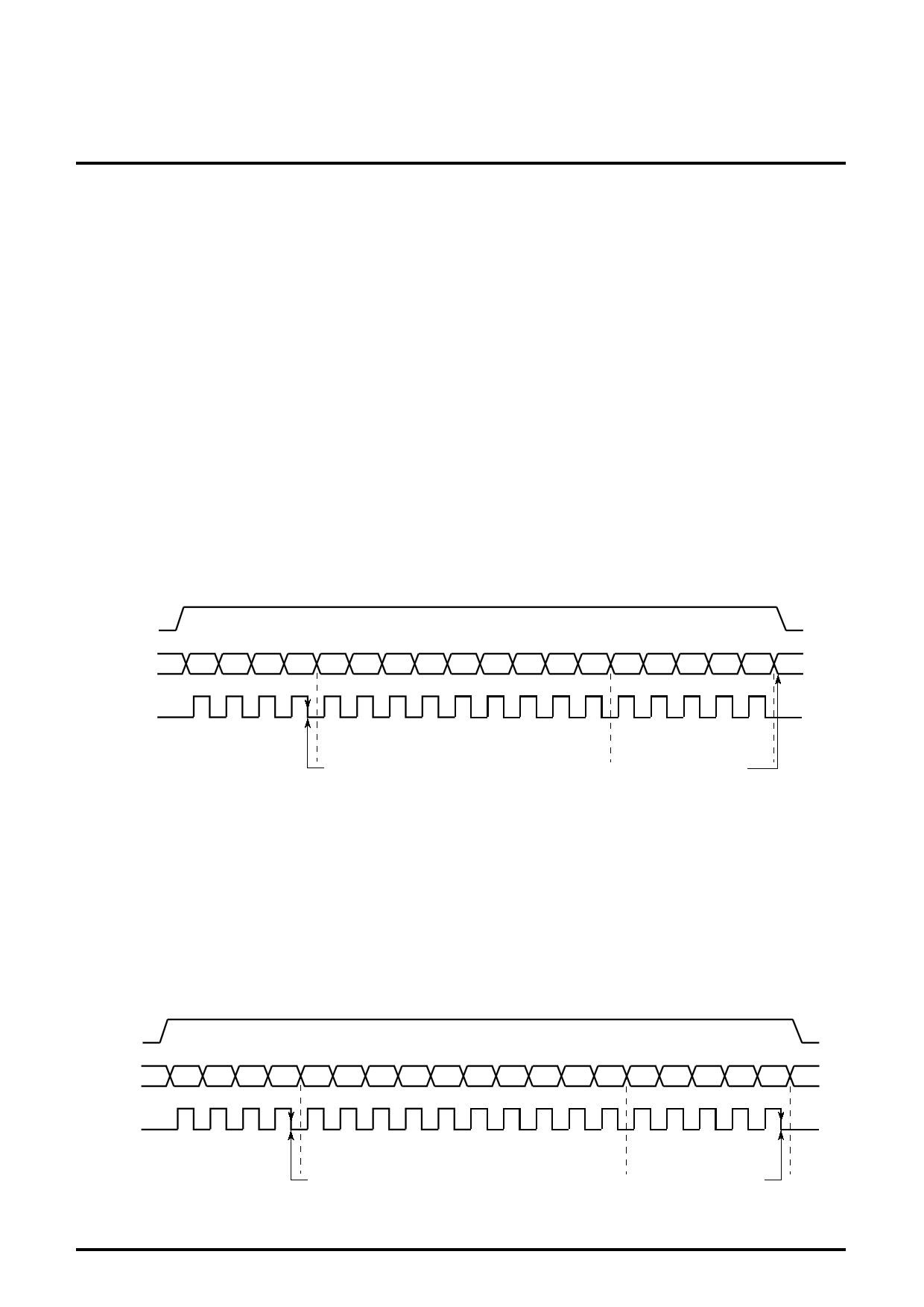
(1) Transfer of the 18th bit data (CONT terminal is "L" )
Data is latched by the fall of the enable signal after the 18th clock
signal. At this time, the divider of the 1/512 of the reference
frequency is used.
ENA
DATA
CLK
BS4 BS3 BS2 BS1 28 27 26 25 24 23 22 21 20 24 23 22 21 20
M8 M7 M6 M5 M4 M3 M2 M1 M0 S4 S3 S2 S1 S0
BAND SW
DATA
M COUNTER DIVIDER
RATIO SETTING
READ INTO LATCH
S COUNTER DIVIDER
RATIO SETTING
READ INTO LATCH
(2) Transfer of the 19th bit data (CONT terminal is "L" or "open")
The data is latched at the 19th pulse of the clock signal.
Reference frequency divider ratio is established in 1/1024 in case of
"L" CONT terminal at this time.
Reference frequency divider ratio is established in 1/640 in case of
"opening" CONT terminal.
Invalid the clock signal after 19th pulse.
Notice) When CONT terminal is "L", to change reference frequency,
set up as ENA in "L" after 19th pulse of clock signal by all means.
ENA
DATA
CLK
BS4 BS3 BS2 BS1 29 28 27 26 25 24 23 22 21 20 24 23 22 21 20
M9 M8 M7 M6 M5 M4 M3 M2 M1 M0 S4 S3 S2 S1 S0
BAND SW
DATA
M COUNTER DIVIDER
RATIO SETTING
READ INTO LATCH
S COUNTER DIVIDER
RATIO SETTING
READ INTO LATCH
5
5 Page | ||
| Páginas | Total 8 Páginas | |
| PDF Descargar | [ Datasheet M64898GP.PDF ] | |
Hoja de datos destacado
| Número de pieza | Descripción | Fabricantes |
| M64898GP | PLL FREQUENCY SYNTHESIZER WITH DC-DC CONVERTER FOR PC | Mitsubishi |
| Número de pieza | Descripción | Fabricantes |
| SLA6805M | High Voltage 3 phase Motor Driver IC. |
Sanken |
| SDC1742 | 12- and 14-Bit Hybrid Synchro / Resolver-to-Digital Converters. |
Analog Devices |
|
DataSheet.es es una pagina web que funciona como un repositorio de manuales o hoja de datos de muchos de los productos más populares, |
| DataSheet.es | 2020 | Privacy Policy | Contacto | Buscar |
