|
|
|
PDF M5M29GT160BVP Data sheet ( Hoja de datos )
| Número de pieza | M5M29GT160BVP | |
| Descripción | 16 /777 /216-BIT (2097 /152-WORD BY 8-BIT / 1048 /576-WORD BY16-BIT)CMOS 3.3V-ONLY / BLOCK ERASE FLASH MEMORY | |
| Fabricantes | Mitsubishi | |
| Logotipo | ||
Hay una vista previa y un enlace de descarga de M5M29GT160BVP (archivo pdf) en la parte inferior de esta página. Total 25 Páginas | ||
|
No Preview Available !
MITSUBISHI LSIs
M5M29GB/T160BVP-80
16,777,216-BIT (2097,152-WORD BY 8-BIT / 1048,576-WORD BY16-BIT)
CMOS 3.3V-ONLY, BLOCK ERASE FLASH MEMORY
DESCRIPTION
The MITSUBISHI Mobile FLASH M5M29GB/T160BVP are 3.3V-only high speed 16,777,216-bit CMOS boot block Flash Memories with
alternating BGO (Back Ground Operation) feature. The BGO feature of the device allows Program or Erase operations to be performed in
one bank while the device simultaneously allows Read operations to be performed on the other bank. This BGO feature is suitable for
mobile and personal computing, and communication products. The M5M29GB/T160BVP are fabricated by CMOS technology for the
peripheral circuits and DINOR(Divided bit line NOR) architecture for the memory cells, and are available in in 48pin TSOP(I) .
FEATURES
Organization
.................................1048,576 word x 16bit
.................................2,097,152 word x 8 bit
Supply voltage ............................................................. VCC = 2.7~3.6V
Access time
.............................. 80ns (Vcc=3.3V+/-0.3V)
90ns (Vcc=2.7~3.6V)
Power Dissipation
Read
.................................
54 mW (Max. at 5MHz)
(After Automatic Power saving) .......... 0.33mW (typ.)
Program/Erase
Standby
..................................................................102.633mmWW
(Max.)
(typ.)
Deep power down mode ....................... 0.33mW (typ.)
Auto program for Bank(I)
Program Time .................................4ms (typ.)
Program Unit
(Byte Program)
(Page Program)
..................................................11w28owrdo/1rdb/y2t5e6byte
Auto program for Bank(II)
Program Time .................................4ms (typ.)
Program Unit ................................. 128word/256byte
Auto Erase
Erase time
................................. 40 ms (typ.)
Erase Unit
Bank(I)
Bank(II)
PBMaoaroiantmBBellotoeccrkkBl.o...c...k..................................................311266KKKwwwooorrrddd///633422KKKbbbyyyttteee
x
x
x
1
7
28
.........................................
Program/Erase cycles
100Kcycles
Boot Block
M5M29GB160BVP ........................ Bottom Boot
M5M29GT160BVP ........................ Top Boot
Other Functions
Soft Ware Command Control
Selective Block Lock
Erase Suspend/Resume
Program Suspend/Resume
Status Register Read
Alternating Back Ground Program/Erase Operation
Between Bank(I) and Bank(II)
Package
48-Lead, 12mm x 20mm TSOP (type-I)
APPLICATION
Code Strage
Digital Cellular Phone
Telecommunication
Mobile Computing Machine
PDA (Personal Digital Assistance)
Car Navigation System
Video Game Machine
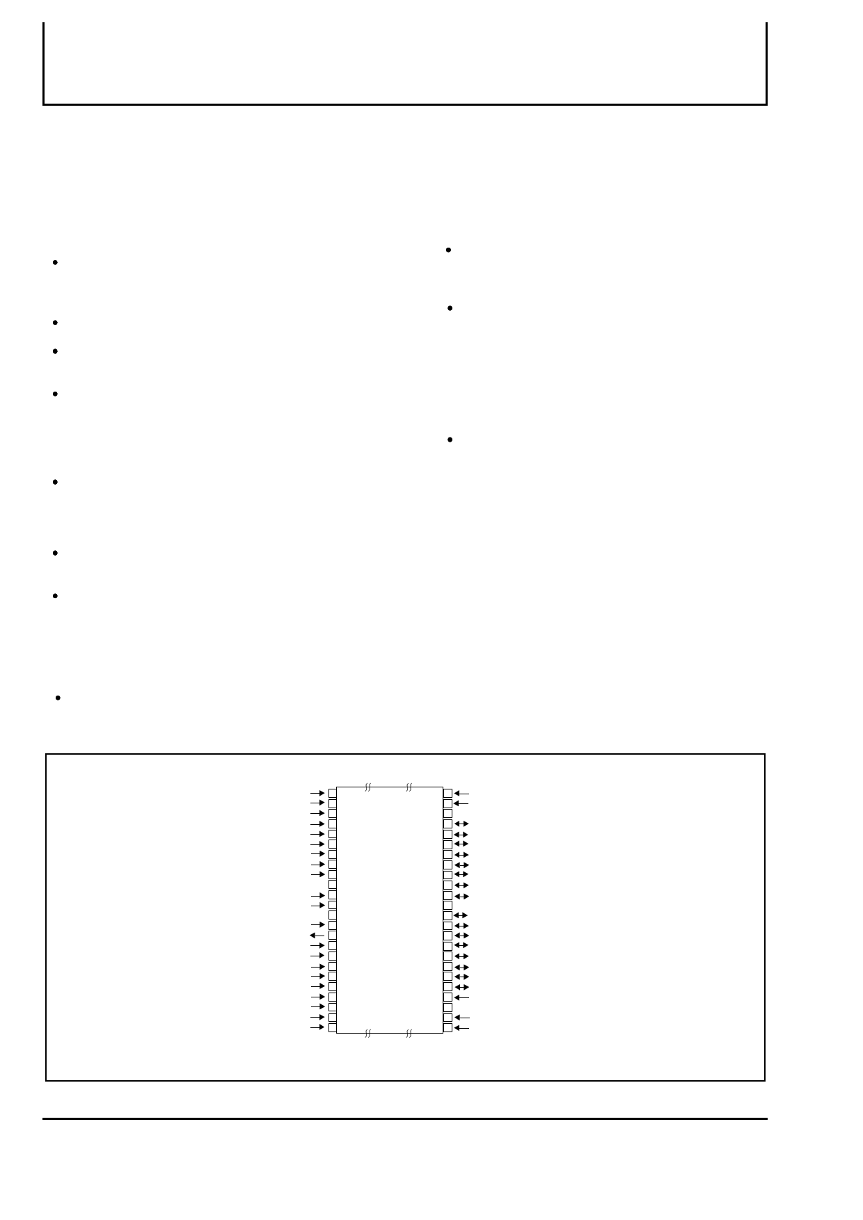
PIN CONFIGURATION (TOP VIEW)
160BVP
A15
A14
A13
A12
A11
A10
A9
A8
A19
NC
WE#
RP#
NC
WP#
RY/BY#
A18
A17
A7
A6
A5
A4
A3
A2
A1
1
2
3
4
5
6
7
8
9
10
11
12
13
14
15
16
17
18
19
20
21
22
23
24
M5M29GB/T
160BVP
160BVP
48 A16
47 BYTE#
46 GND
45 DQ15/A-1
44 DQ7
43 DQ14
42 DQ6
41 DQ13
40 DQ5
39 DQ12
38 DQ4
37 VCC
36 DQ11
35 DQ3
34 DQ10
33 DQ2
32 DQ9
31 DQ1
30 DQ8
29 DQ0
28 OE#
27 GND
26 CE#
25 A0
Outline 48pin TSOP type-I (12 X 20mm)
VP(Normal bend)
NC : NO CONNECTION
1 Sep 1999. Rev2.0
1 page 
MITSUBISHI LSIs
M5M29GB/T160BVP-80
16,777,216-BIT (2097,152-WORD BY 8-BIT / 1048,576-WORD BY16-BIT)
CMOS 3.3V-ONLY, BLOCK ERASE FLASH MEMORY
Mitsubishi 16M Flash Memory Type name
M 5 M 29G T 160B VP
Operating Voltage :
29G : 2.7 - 3.6V
Standard / BGO Type
29W : 1.65 - 2.2V
Standard / BGO Type
Boot Block :
T : Top Boot
B : Bottom Boot
Density/Write Protect/
Word Organizetion:
160B : 16M WP#, x8/x16
161B : 16M WP1# & WP2#, x16
Package :
VP : 48pin TSOP(I) 12mm x 20mm (Nomal Pinout)
WG: CSP Ball Pitch 0.75mm,6x8 array, 7mm x 8.5mm
5 Sep 1999. Rev2.0
5 Page 
MITSUBISHI LSIs
M5M29GB/T160BVP-80
16,777,216-BIT (2097,152-WORD BY 8-BIT / 1048,576-WORD BY16-BIT)
CMOS 3.3V-ONLY, BLOCK ERASE FLASH MEMORY
AC ELECTRICAL CHARACTERISTICS (Ta = -40 ~85°C)
Read-Only Mode
Symbol
Parameter
tRC
ta (AD)
ta (CE)
ta (OE)
tCLZ
tDF(CE)
tOLZ
tDF(OE)
tPHZ
tAVAV
tAVQV
tELQV
tGLQV
tELQX
tEHQZ
tGLQX
tGHQZ
tPLQZ
Read cycle time
Address access time
Chip enable access time
Output enable access time
Chip enable to output in low-Z
Chip enable high to output in high Z
Output enable to output in low-Z
Output enable high to output in high Z
RP# low to output high-Z
ta(BYTE) tFL/HQV BYTE# access time
tBHZ tFLQZ BYTE# low to output high-Z
tOH tOH Output hold from CE#, OE#, addresses
tBCD tELFL/H F-CE# low to BYTE# high or low
tBAD tAVFL/H Address to BYTE# high or low
tOEH tWHGL OE# hold from WE# high
tPS tPHEL RP# recovery to CE# low
Limits
Speed Item: -80
Vcc=3.3V+/-0.3V
Min Typ Max
80
80
80
30
0
25
0
25
150
Vcc=2.7~3.6V
Min Typ
90
0
0
80
25
00
5
50
10 10
150 150
Timing measurements are made under AC waveforms for read operations.
Max
90
90
30
25
25
150
90
25
5
5
AC ELECTRICAL CHARACTERISTICS (Ta = -40 ~85°C)
Write Mode (WE# control)
Symbol
Parameter
tWC
tAS
tAH
tDS
tDH
tOEH
tRE
tCS
tCH
tWP
tWPH
tBS
tBH
tAVAV Write cycle time
tAVWH Address set-up time
tWHAX Address hold time
tDVWH Data set-up time
tWHDX Data hold time
tWHGL OE# hold from WE# high
- Latency between Read and Write FFH or 71H
tELWL Chip enable set-up time
tWHEH Chip enable hold time
tWLWH Write pulse width
tWHWL Write pulse width high
tFL/HWH Byte enable high or low set-up time
tWHFL/H Byte enable high or low hold time
tGHWL tGHWL OE# hold to WE# Low
tBLS tPHHWH Block Lock set-up to write enable high
tBLH tQVPH Block Lockhold from valid SRD
tDAP tWHRH1 Duration of auto-program operation
tDAE tWHRH2 Duration of auto-block erase operation
tWHRL tWHRL Write enable high to F-RY/BY# low
tPS tPHWL RP# high recovery to write enable low
Limits
Speed Item: -80
Vcc=3.3V+/-0.3V
Vcc=2.7~3.6V
Min Typ Max Min Typ
80 90
50 50
00
50 50
00
10 10
30 30
00
00
60 60
30 30
50 50
80 90
00
80 90
00
4 80
4
40 600
90
40
150 150
Read timing parameters during command write operations mode are the same as during read-only operations mode.
Typical values at Vcc=3.3V, Ta=25°C
Max
80
600
90
Unit
ns
ns
ns
ns
ns
ns
ns
ns
ns
ns
ns
ns
ns
ns
ns
ns
Unit
ns
ns
ns
ns
ns
ns
ns
ns
ns
ns
ns
ns
ns
ns
ns
ns
ms
ms
ns
ns
11 Sep 1999. Rev2.0
11 Page | ||
| Páginas | Total 25 Páginas | |
| PDF Descargar | [ Datasheet M5M29GT160BVP.PDF ] | |
Hoja de datos destacado
| Número de pieza | Descripción | Fabricantes |
| M5M29GT160BVP | 16 /777 /216-BIT (2097 /152-WORD BY 8-BIT / 1048 /576-WORD BY16-BIT)CMOS 3.3V-ONLY / BLOCK ERASE FLASH MEMORY | Mitsubishi |
| M5M29GT160BVP-80 | 16 /777 /216-BIT (2097 /152-WORD BY 8-BIT / 1048 /576-WORD BY16-BIT)CMOS 3.3V-ONLY / BLOCK ERASE FLASH MEMORY | Mitsubishi |
| Número de pieza | Descripción | Fabricantes |
| SLA6805M | High Voltage 3 phase Motor Driver IC. |
Sanken |
| SDC1742 | 12- and 14-Bit Hybrid Synchro / Resolver-to-Digital Converters. |
Analog Devices |
|
DataSheet.es es una pagina web que funciona como un repositorio de manuales o hoja de datos de muchos de los productos más populares, |
| DataSheet.es | 2020 | Privacy Policy | Contacto | Buscar |