|
|
|
PDF M29F040 Data sheet ( Hoja de datos )
| Número de pieza | M29F040 | |
| Descripción | 4 Mbit 512Kb x8 / Uniform Block Single Supply Flash Memory | |
| Fabricantes | ST Microelectronics | |
| Logotipo | ||
Hay una vista previa y un enlace de descarga de M29F040 (archivo pdf) en la parte inferior de esta página. Total 30 Páginas | ||
|
No Preview Available !
M29F040
4 Mbit (512Kb x8, Uniform Block) Single Supply Flash Memory
M29F040 is replaced by the M29F040B
5V ± 10% SUPPLY VOLTAGE for PROGRAM,
ERASE and READ OPERATIONS
FAST ACCESS TIME: 70ns
BYTE PROGRAMMING TIME: 10µs typical
ERASE TIME
– Block: 1.0 sec typical
– Chip: 2.5 sec typical
PROGRAM/ERASE CONTROLLER (P/E.C.)
– Program Byte-by-Byte
– Data Polling and Toggle bits Protocol for
P/E.C. Status
MEMORY ERASE in BLOCKS
– 8 Uniform Blocks of 64 KBytes each
– Block Protection
– Multiblock Erase
ERASE SUSPEND and RESUME MODES
LOW POWER CONSUMPTION
– Read mode: 8mA typical (at 12MHz)
– Stand-by mode: 25µA typical
– Automatic Stand-by mode
100,000 PROGRAM/ERASE CYCLES per
BLOCK
20 YEARS DATA RETENTION
– Defectivity below 1ppm/year
ELECTRONIC SIGNATURE
– Manufacturer Code: 20h
– Device Code: E2h
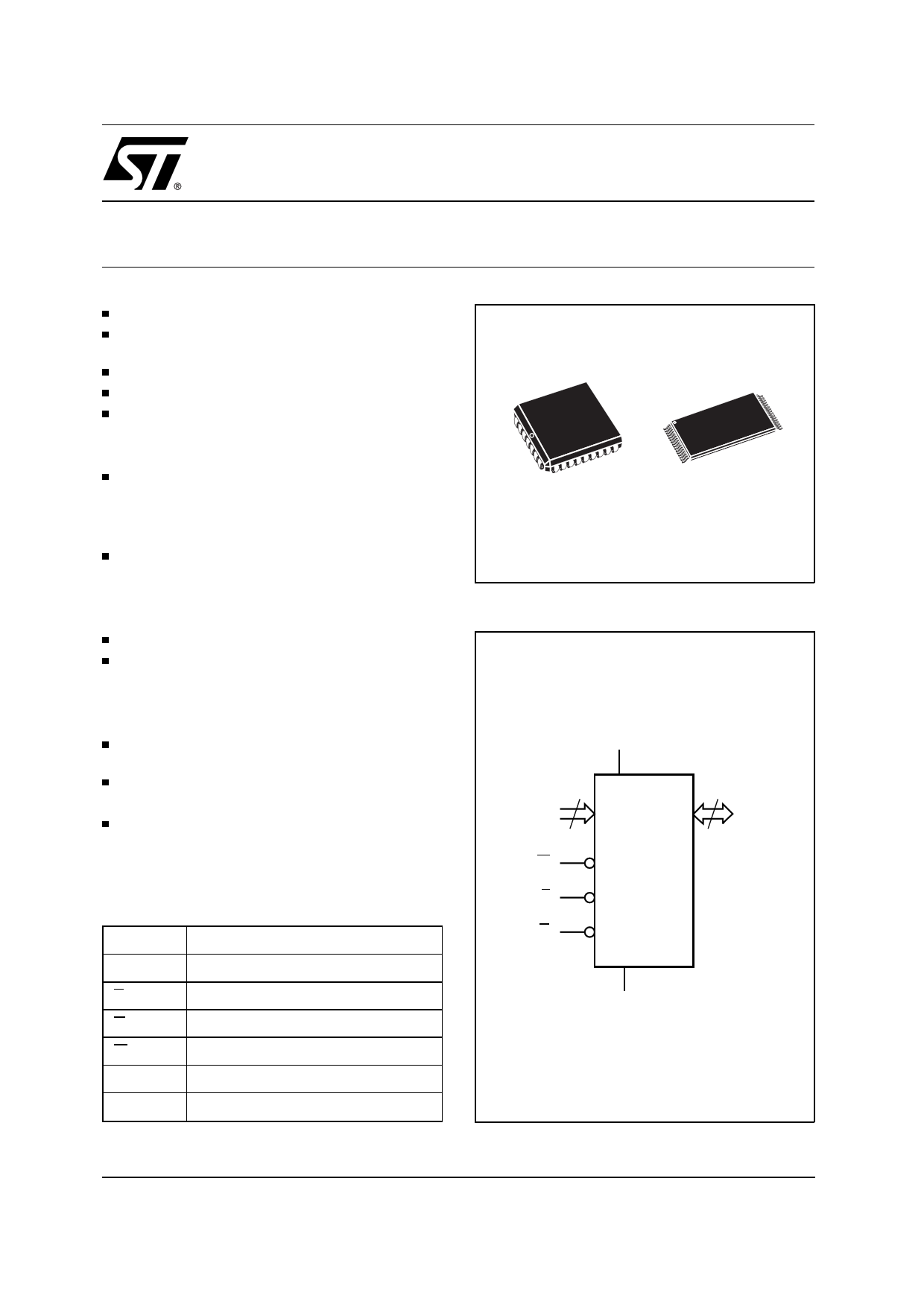
Table 1. Signal Names
A0-A18
Address Inputs
DQ0-DQ7 Data Input / Outputs
E Chip Enable
G Output Enable
W Write Enable
VCC Supply Voltage
VSS Ground
NOT FOR NEW DESIGN
PLCC32 (K)
TSOP32 (N)
8 x 20 mm
Figure 1. Logic Diagram
VCC
19
A0-A18
8
DQ0-DQ7
W M29F040
E
G
VSS
AI01372
November 1999
This is information on a product still in production but not recommended for new designs.
1/31
1 page 
M29F040
Table 6. Instructions (1,2)
Mne.
Instr. Cyc.
1st Cyc. 2nd Cyc. 3rd Cyc. 4th Cyc. 5th Cyc. 6th Cyc. 7th Cyc.
RST (4,10)
Read Array/
Reset
Addr. (3,7)
1+
Data
X
Read Memory Array until a new write cycle is initiated.
F0h
Addr. (3,7) 5555h
3+
Data
AAh
2AAAh
55h
5555h Read Memory Array until a new write
cycle is initiated.
F0h
Read
RSIG (4) Electronic
Signature
Addr. (3,7) 5555h
3+
Data
AAh
2AAAh
55h
5555h Read Electronic Signature until a new
write cycle is initiated. See Note 5.
90h
RBP (4)
Read Block
Protection
Addr. (3,7) 5555h
3+
Data
AAh
2AAAh
55h
5555h Read Block Protection until a new write
cycle is initiated. See Note 6.
90h
PG Program
Addr. (3,7) 5555h
4
Data
AAh
2AAAh
55h
5555h
A0h
Program
Address Read Data Polling or Toggle Bit
until Program completes.
Program
Data
BE Block Erase
Addr. (3,7) 5555h
6
2AAAh
5555h
5555h
2AAAh
Block Additional
Address Block (8)
Data
AAh 55h 80h AAh 55h 30h
30h
CE Chip Erase
Addr. (3,7) 5555h
6
Data
AAh
2AAAh
55h
5555h
80h
5555h
AAh
2AAAh
55h
5555h
10h
Note 9
ES
Erase
Suspend
Addr. (3,7)
1
Data
X Read until Toggle stops, then read all the data needed from any
uniform block(s) not being erased then Resume Erase.
B0h
ER
Erase
Resume
Addr. (3,7)
1
Data
X Read Data Polling or Toggle Bit until Erase completes or Erase
is suspended another time
30h
Notes: 1. Command not interpreted in this table will default to read array mode.
2. While writing any command or during RSG and RSP execution, the P/E.C. can be reset by writing the command 00h to the C.I.
3. X = Don’t Care.
4. The first cycle of the RST, RBP or RSIG instruction is followed by read operations to read memory array, Status Register or
Electronic Signature codes. Any number of read cycles can occur after one command cycle.
5. Signature Address bits A0, A1, A6 at VIL will output Manufacturer code (20h). Address bits A0 at VIH and A1, A6 at VIL will output
Device code.
6. Protection Address: A0, A6 at VIL, A1 at VIH and A16, A17, A18 within the uniform block to be checked, will output the Block Protection
status.
7. Address bits A15-A18 are don’t care for coded address inputs.
8. Optional, additional blocks addresses must be entered within a 80µs delay after last write entry, timeout status can be verified
through DQ3 value. When full command is entered, read Data Polling or Toggle bit until Erase is completed or suspended.
9. Read Data Polling or Toggle bit until Erase completes.
10. A wait time of 5µs is necessary after a Reset command, if the memory is in a Block Erase status, before starting
any operation.
5/31
5 Page 
M29F040
Table 12A. Read AC Characteristics
(TA = 0 to 70°C, –20 to 85°C, –40 to 85°C or –40 to 125°C)(3)
M29F040
Symbol Alt
Parameter
Test Condition
-70 -90
VCC = 5V ± 5% VCC = 5V ± 10% Unit
Standard
Interface
Standard
Interface
Min Max Min Max
tAVAV tRC Address Valid to Next Address Valid E = VIL, G = VIL 70
90 ns
tAVQV tACC Address Valid to Output Valid
E = VIL, G = VIL
70
90 ns
tELQX (1) tLZ Chip Enable Low to Output Transition
G = VIL
0
0 ns
tELQV (2) tCE Chip Enable Low to Output Valid
G = VIL
70 90 ns
tGLQX (1)
tOLZ
Output Enable Low to Output
Transition
E = VIL
0
0 ns
tGLQV (2) tOE Output Enable Low to Output Valid
E = VIL
30 35 ns
tEHQX
tOH
Chip Enable High to Output
Transition
G = VIL
0
0 ns
tEHQZ (1) tHZ Chip Enable High to Output Hi-Z
G = VIL
20 20 ns
tGHQX
tOH
Output Enable High to Output
Transition
E = VIL
0
0
tGHQZ (1) tDF Output Enable High to Output Hi-Z
E = VIL
20 20
tAXQX
tOH
Address Transition to Output
Transition
E = VIL, G = VIL 20
20
Notes: 1. Sampled only, not 100% tested.
2. G may be delayed by up to tELQV - tGLQV after the falling edge of E without increasing tELQV.
3. The temperature range –40 to 125°C is guaranteed at 70ns with High Speed Interface test condition and VCC = 5V ± 5%.
ns
ns
ns
Block Erase (BE) instruction. This instruction
uses a minimum of six write cycles. The Erase
Set-up command 80h is written to address 5555h
on third cycle after the two coded cycles. The Block
Erase Confirm command 30h is written on sixth
cycle after another two coded cycles. During the
input of the second command an address within
the block to be erased is given and latched into the
memory. Additional Block Erase confirm com-
mands and block addresses can be written sub-
sequently to erase other blocks in parallel, without
further coded cycles. The erase will start after an
Erase timeout period of about 100µs. Thus, addi-
tional Block Erase commands must be given within
this delay. The input of a new Block Erase com-
mand will restart the timeout period. The status of
the internal timer can be monitored through the
level of DQ3, if DQ3 is ’0’ the Block Erase Com-
mand has been given and the timeout is running, if
DQ3 is ’1’, the timeout has expired and the P/E.C
is erasing the block(s). Before and during Erase
timeout, any command different from 30h will abort
the instruction and reset the device to read array
mode. It is not necessary to program the block with
00h as the P/E.C. will do this automatically before
erasing to FFh. Read operations after the sixth
rising edge of W or E output the status register bits.
During the execution of the erase by the P/E.C., the
memory accepts only the ES (Erase Suspend) and
RST (Reset) instructions. Data Polling bit DQ7
returns ’0’ while the erasure is in progress and ’1’
when it has completed. The Toggle Bit DQ6 toggles
during the erase operation. It stops when erase is
completed. After completion the Status Register
bit DQ5 returns ’1’ if there has been an Erase
Failure because erasure has not completed even
after the maximum number of erase cycles have
been executed. In this case, it will be necessary to
input a Reset (RST) to the command interface in
order to reset the P/E.C.
11/31
11 Page | ||
| Páginas | Total 30 Páginas | |
| PDF Descargar | [ Datasheet M29F040.PDF ] | |
Hoja de datos destacado
| Número de pieza | Descripción | Fabricantes |
| M29F040 | 4 Mbit 512Kb x8 / Uniform Block Single Supply Flash Memory | ST Microelectronics |
| M29F040B | 4 Mbit 512Kb x8 / Uniform Block Single Supply Flash Memory | ST Microelectronics |
| Número de pieza | Descripción | Fabricantes |
| SLA6805M | High Voltage 3 phase Motor Driver IC. |
Sanken |
| SDC1742 | 12- and 14-Bit Hybrid Synchro / Resolver-to-Digital Converters. |
Analog Devices |
|
DataSheet.es es una pagina web que funciona como un repositorio de manuales o hoja de datos de muchos de los productos más populares, |
| DataSheet.es | 2020 | Privacy Policy | Contacto | Buscar |