|
|
|
PDF LCX029CPT Data sheet ( Hoja de datos )
| Número de pieza | LCX029CPT | |
| Descripción | 2.3cm (0.9 Type) Black-and-White LCD Panel | |
| Fabricantes | Sony | |
| Logotipo | ||
Hay una vista previa y un enlace de descarga de LCX029CPT (archivo pdf) en la parte inferior de esta página. Total 27 Páginas | ||
|
No Preview Available !
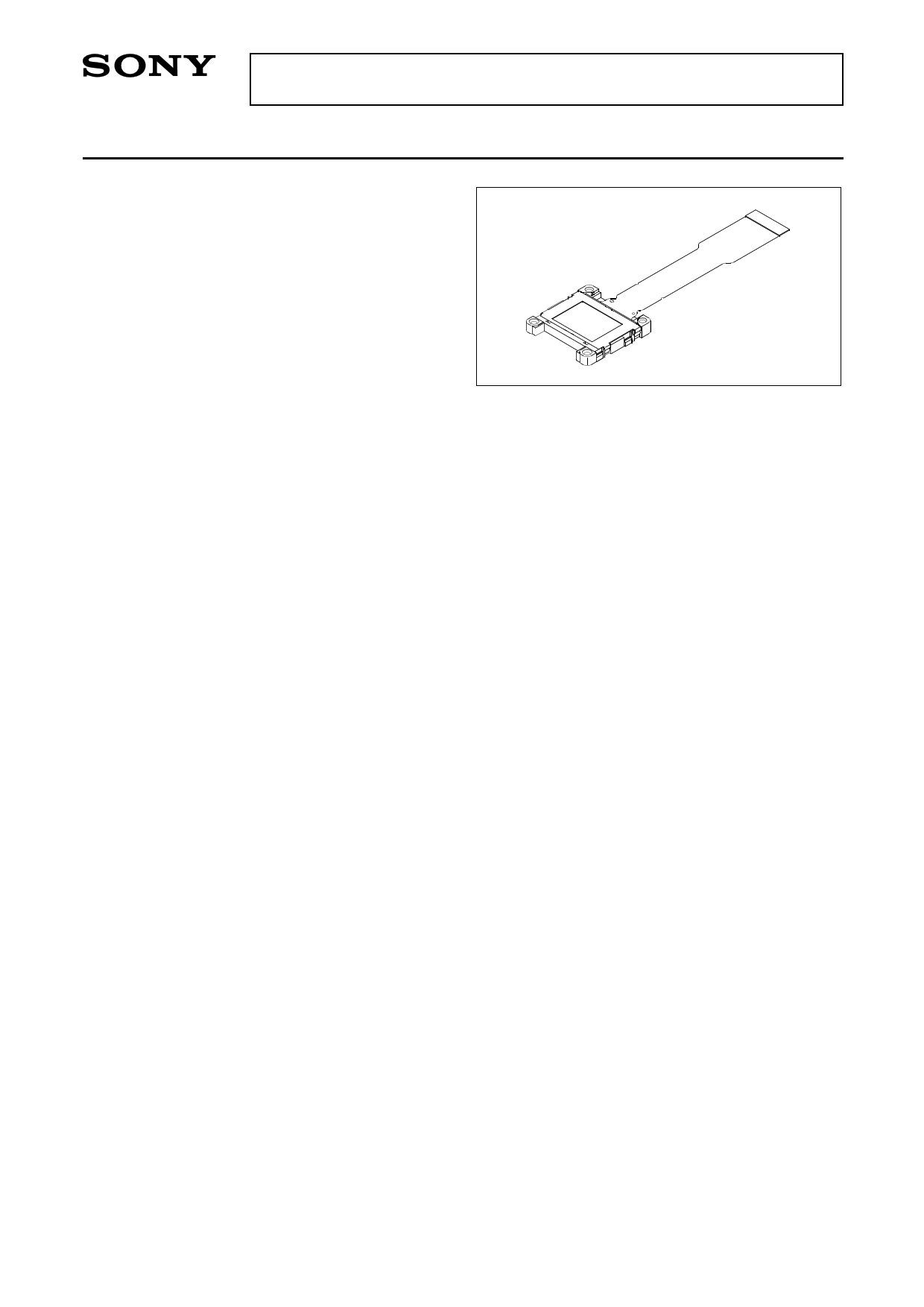
LCX029CPT
2.3cm (0.9 Type) Black-and-White LCD Panel
Description
The LCX029CPT is a 2.3cm diagonal active matrix
TFT-LCD panel addressed by polycrystalline silicon
super thin film transistors with a built-in peripheral
driving circuit. Use of three LCX029CPT panels
provides a full-color representation. The striped
arrangement suitable for data projectors is capable
of displaying fine text and vertical lines.
The adoption of DMS∗1 structure and high light
resistance structure realize a high luminance screen.
And cross talk free circuit and ghost free circuit
contribute to high picture quality.
This panel has a polysilicon TFT high-speed scanner
and built-in function to display images up/down and/or
right/left inverse. The built-in 5V interface circuit leads
to lower voltage of timing and control signals.
The panel contains an active area variable circuit
which supports S-XGA 5:4 and PC-98 8:5 data signals
by changing the active area according to the type of
input signal.
∗1 Dual Metal Shield
Features
• Number of active dots: 786,432 (0.9 Type, 2.3cm in diagonal)
• XGA, SVGA, VGA, NTSC, PAL display
• SXGA display with simple display
• High optical transmittance: 16% (typ.)
• Built-in cross talk free circuit and ghost free circuit
• High contrast ratio with normally white mode: 400 (typ.)
• Built-in H and V drivers (built-in input level conversion circuit, 5V driving possible)
• Up/down and/or right/left inverse display function
• Antidust glass package
• Left twist liquid crystal
Element Structure
• Dots: 1024 (H) × 768 (V) = 786,432
• Built-in peripheral driver using polycrystalline silicon super thin film transistors
Applications
• Liquid crystal data projectors
• Liquid crystal multimedia projectors
• Liquid crystal rear-projector TVs, etc.
∗ The company's name and product's name in this data sheet is a trademark or a registered trademark of each company.
Sony reserves the right to change products and specifications without prior notice. This information does not convey any license by
any implication or otherwise under any patents or other right. Application circuits shown, if any, are typical examples illustrating the
operation of the devices. Sony cannot assume responsibility for any problems arising out of the use of these circuits.
–1–
E00457C18
1 page 
LCX029CPT
Input Equivalent Circuit
To prevent static charges, protective diodes are provided for each pin except the power supplies. In addition,
protective resistors are added to all pins except the video signal inputs. All pins are connected to VSS with a
high resistor of 1MΩ (typ.). The equivalent circuit of each input pin is shown below: (Resistance value: typ.)
(1) VSIG1 to VSIG12, PSIG
HVDD
Input
1MΩ
(2) HCK1, HCK2
(3) RGT
Input
HVDD
250Ω
250Ω
1MΩ
Signal line
250Ω
250Ω
1MΩ
Level conversion circuit
(2-phase input)
Input
HVDD
2.5kΩ
2.5kΩ
1MΩ
Level conversion circuit
(single-phase input)
(4) HST
Input
HVDD
250Ω
250Ω
1MΩ
Level conversion circuit
(single-phase input)
(5) PCG, VCK
Input
VVDD
250Ω
250Ω
1MΩ
Level conversion circuit
(single-phase input)
(6) VST, BLK, ENB, HB, DWN
Input
VVDD
2.5kΩ
2.5kΩ
1MΩ
Level conversion circuit
(single-phase input)
(7) VB
VVDD
Input
400kΩ
LC
(8) COM
VVDD
Input
1MΩ
–5–
LC
are all Vss.
5 Page 
LCX029CPT
Electrical Characteristics (Ta = 25°C, HVDD = 13.5V, VVDD = 15.5V)
1. Horizontal drivers
Item
Symbol Min. Typ. Max. Unit
Condition
Input pin capacitance HCKn
CHckn — 15 20 pF
HST
CHst — 15 20 pF
Input pin current
HCK1
–500 –200 — µA HCK1 = GND
HCK2
–1000 –300 — µA HCK2 = GND
HST
–500 –150 — µA HST = GND
RGT
–150 –40 — µA RGT = GND
Video signal input pin capacitance Csig — 50 200 pF
Current consumption
IH — 10.0 15.0 mA HCKn: HCK1, HCK2 (3.9MHz)
2. Vertical drivers
Item
Symbol Min. Typ. Max. Unit
Condition
Input pin capacitance VCK
CVck — 15 20 pF
VST
CVst
— 15 20 pF
Input pin current
VCK,PCG
–1000 –150 — µA VCK = GND, PCG = GND
VST, ENB, DWN, BLK, HB,
VB
–150 –30 —
µA
VST, ENB, DWN,BLK, HB
VB = GND
Current consumption
IV — 3.0 6.0 mA VCK: (34.3kHz)
3. Total power consumption of the panel
Item Symbol Min. Typ. Max. Unit
Total power consumption of the panel PWR — 200 350 mW
4. Pin input resistance
Item
Pin – VSS input resistance
Symbol Min. Typ. Max. Unit
Rpin 0.4 1 — MΩ
5. Uniformity improvement signal
Item Symbol Min. Typ. Max. Unit
Input pin capacitance for uniformity
improvement signal
CPSIGo
—
11
16
nF
6. COM pin capacitance
Item
COM pin capacitance
Symbol Min. Typ. Max. Unit
COM — 17 25 nF
– 11 –
11 Page | ||
| Páginas | Total 27 Páginas | |
| PDF Descargar | [ Datasheet LCX029CPT.PDF ] | |
Hoja de datos destacado
| Número de pieza | Descripción | Fabricantes |
| LCX029CPT | 2.3cm (0.9 Type) Black-and-White LCD Panel | Sony |
| Número de pieza | Descripción | Fabricantes |
| SLA6805M | High Voltage 3 phase Motor Driver IC. |
Sanken |
| SDC1742 | 12- and 14-Bit Hybrid Synchro / Resolver-to-Digital Converters. |
Analog Devices |
|
DataSheet.es es una pagina web que funciona como un repositorio de manuales o hoja de datos de muchos de los productos más populares, |
| DataSheet.es | 2020 | Privacy Policy | Contacto | Buscar |