|
|
|
PDF KA3524 Data sheet ( Hoja de datos )
| Número de pieza | KA3524 | |
| Descripción | SMPS Controller | |
| Fabricantes | Fairchild | |
| Logotipo | ||
Hay una vista previa y un enlace de descarga de KA3524 (archivo pdf) en la parte inferior de esta página. Total 12 Páginas | ||
|
No Preview Available !
KA3524
SMPS Controller
www.fairchildsemi.com
Features
• Complete PWM power control circuit
• Operation beyond 100KHz
• 2% frequency stability with temperature
• Total quiescent current less than 10mA
• Single ended or push-pull outputs
• Current limit amplifier provides external component
protection
• On-chip protection against excessive junction temperature
and output current
• 5V, 50mA linear regulator output available to user
Description
The KA3524 regulating pulse width modulator contains
all of the control circuit necessary to implement switching
regulators of either polarity, transformer coupled DC to
DC converters, transformerless polarity converters and volt-
age doublers, as well as other power control applications.
This device includes a 5V voltage regulator capable of sup-
plying up to 50mA to external circuit , a control ampli-
fier, an oscillator, a pulse width modulator, a phase
splitting flip-flop, dual alternating output switch transistors,
and current limiting and shut-down circuit. Both the regu-
lator output transistor and each output switch are internally
current limiting and, to limit junction temperature, aninter-
nal thermal shutdown circuit is employed.
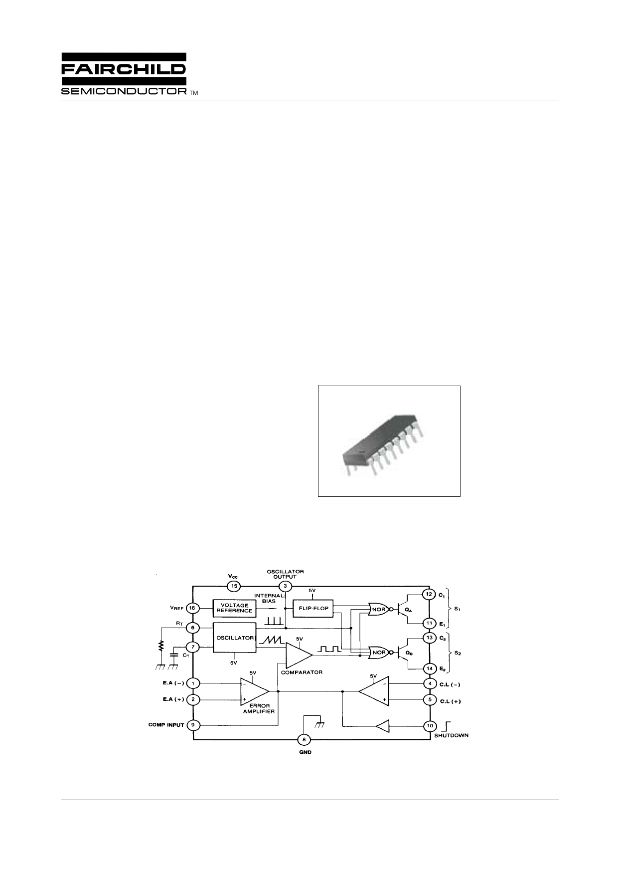
16-DIP
Internal Block Diagram
1
©2000 Fairchild Semiconductor International
Rev. 5.0
1 page 
KA3524
Error Amplifier
This circuit is a simple differential-input, transconductance amplifier. The output is the compensation terminal pin 9, which is
a high impedance node (RL:=5MΩ). The gain is
GV = gmRL = 8----I--L---R-----L- = 0.002 RL
2KT
and can easily be reduced from a nominal of 10,000 by an external shunt resistance from pin 9 to ground, as shown in Figure
8,In addition to DC gain control, the compensation terminal is also the place for AC phase compensation. The frequency
response curves of Figure 5 show the uncompensated amplifier with a single pole at approximately 200Hz and a unity gain
cross-over frequency at 5MHz.typically, most output filter designs will introduce one or more addition poles at a significantly
higher power frequency. Therefore, the best stabilizing network is a series R-C combination between pin 9 and ground which
introduces a zero to cancel one of the output filter poles. A good starting point is 50KΩ plus 0.001 micro farad. One final point
on the compensation terminal is that this is also a convenient place to insert any programming signal which is to override the
error amplifier. Internal shutdown and current limit circuits are connected here, but any other circuit which can sink 200uA
can pull this point to ground, thus shutting off both outputs. While feedback is normally applied around the entire regulator, the
error amplifier can be used with conventional operational amplifier feedback and is stable in either the inverting or non-
inverting mode. Regardless of the connections, however, input common-mode limits must be observed or output sign inver-
sions may happen. For conventional regulator applications, the 5 volt reference voltage must be divided down as shown in Fig-
ure 3. The error amplifier may also be used in fixed duty cycle applications by using the unity gain configuration shown in the
open loop test circuit.
Current Limiting
The current limiting circuitry of the KA3524 is shown in Figure 4.
By matching the base-emitter voltages of Q1 and Q2, and assuming negligible voltage drop across R 1 :
Threshold = VBE(Q1) + I 1R 2 - V BE(Q2)
= l 1R 2 = 200mV
Although this circuit provides a relatively small threshold with a negligible temperature coefficient, there are some limitations
to its use, the most important of which is the ±1 volt common mode range which requires sensing in the ground line. Another
factor to consider is that the frequency compensation provided by R 1C1 and Q1 provides a roll-off pole at approximately
300Hz.Since the gain of this circuit is relatively low, there is a transition region as the current limit amplifier takes over pulse
width control from the error amplifier. For testing purposes, the threshold is defined as the input voltage to get 25% duty cycle
with the error amplifier signaling maximum duty cycle. In addition to constant current limiting, pins 4 and 5 may also be used
in transformer-coupled circuits to sense primary current and shorten an output pulse, should transformer saturation occur.
Another application is to ground pin 5 and use pin 4 as an additional shutdown terminal: i.e., the output will be off with pin 4
open and on when it is grounded. Finally, fold back current limiting can be provided with the network of Figure 5. This cir-
cuit can reduce the short circuit current (lSC)to approximately one third the maximum available output current (I MAX).
Figure 3. Error Amplifier Biasing Circuits
5
5 Page 
Ordering Information
Product Number
KA3524
Package
16-DIP
Operating Temperature
0 ~ 70°C
KA3524
11
11 Page | ||
| Páginas | Total 12 Páginas | |
| PDF Descargar | [ Datasheet KA3524.PDF ] | |
Hoja de datos destacado
| Número de pieza | Descripción | Fabricantes |
| KA3524 | SMPS Controller | Fairchild |
| KA3525A | SMPS CONTROLLER | Fairchild |
| Número de pieza | Descripción | Fabricantes |
| SLA6805M | High Voltage 3 phase Motor Driver IC. |
Sanken |
| SDC1742 | 12- and 14-Bit Hybrid Synchro / Resolver-to-Digital Converters. |
Analog Devices |
|
DataSheet.es es una pagina web que funciona como un repositorio de manuales o hoja de datos de muchos de los productos más populares, |
| DataSheet.es | 2020 | Privacy Policy | Contacto | Buscar |