|
|
|
PDF M50FW080 Data sheet ( Hoja de datos )
| Número de pieza | M50FW080 | |
| Descripción | 8 Mbit 1Mb x8/ Uniform Block 3V Supply Firmware Hub Flash Memory | |
| Fabricantes | ST Microelectronics | |
| Logotipo | ||
Hay una vista previa y un enlace de descarga de M50FW080 (archivo pdf) en la parte inferior de esta página. Total 30 Páginas | ||
|
No Preview Available !
M50FW080
8 Mbit (1Mb x8, Uniform Block)
3V Supply Firmware Hub Flash Memory
s SUPPLY VOLTAGE
– VCC = 3V to 3.6V for Program, Erase and
Read Operations
– VPP = 12V for Fast Program and Fast Erase
(optional)
s TWO INTERFACES
– Firmware Hub (FWH) Interface for embedded
operation with PC Chipsets
– Address/Address Multiplexed (A/A Mux) In-
terface for programming equipment compati-
bility
s FIRMWARE HUB (FWH) HARDWARE
INTERFACE MODE
– 5 Signal Communication Interface supporting
Read and Write Operations
– Hardware Write Protect Pins for Block Pro-
tection
– Register Based Read and Write Protection
– 5 Additional General Purpose Inputs for plat-
form design flexibility
– Synchronized with 33MHz PCI clock
s PROGRAMMING TIME
– 10µs typical
– Quadruple Byte Programming Option
s 16 UNIFORM 64 Kbyte MEMORY BLOCKS
s PROGRAM/ERASE CONTROLLER
– Embedded Byte Program and Block/Chip
Erase algorithms
– Status Register Bits
s PROGRAM and ERASE SUSPEND
– Read other Blocks during Program/Erase
Suspend
– Program other Blocks during Erase Suspend
s FOR USE in PC BIOS APPLICATIONS
s ELECTRONIC SIGNATURE
– Manufacturer Code: 20h
– Device Code: 2Dh
PLCC32 (K)
TSOP40 (N)
10 x 20mm
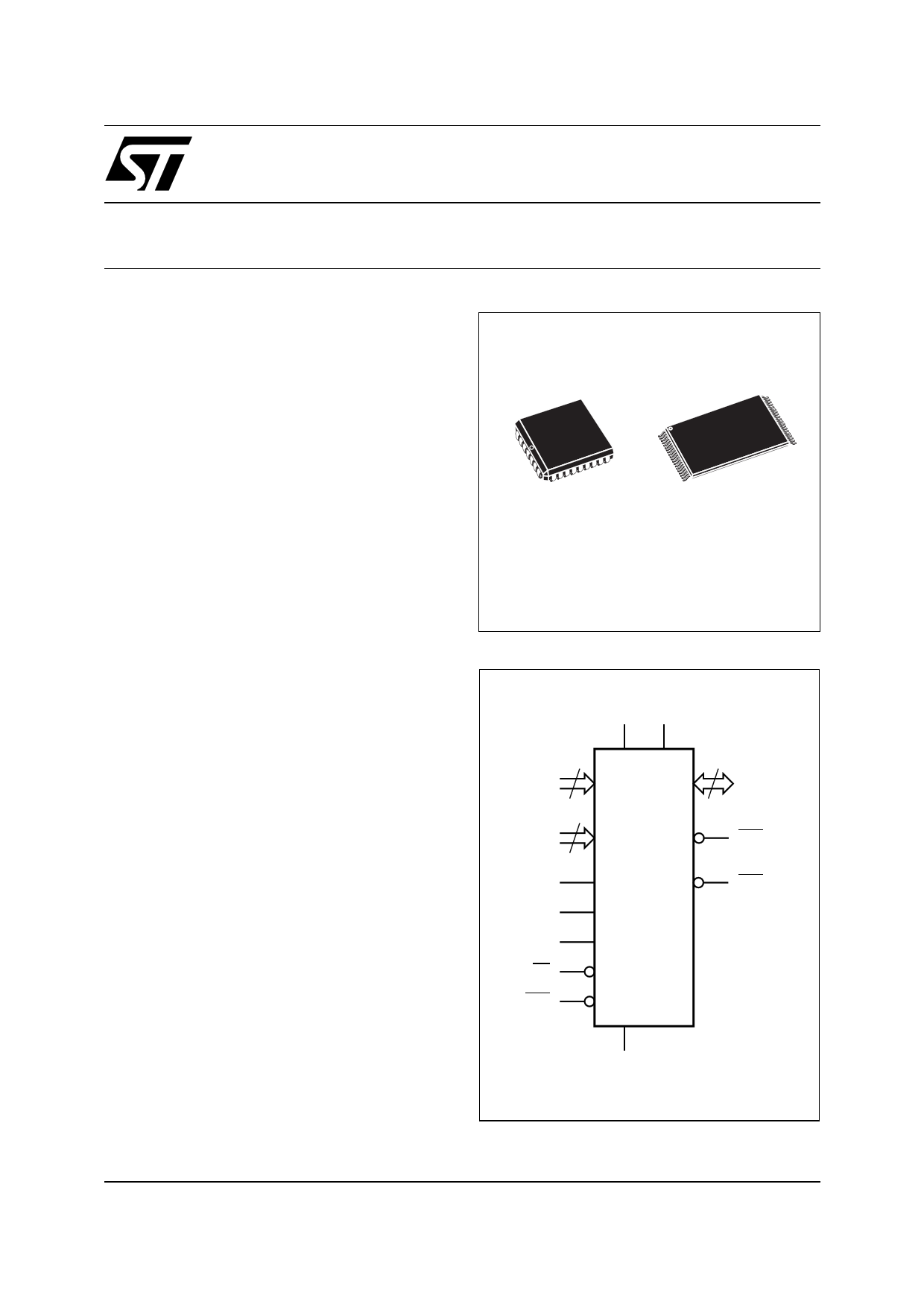
Figure 1. Logic Diagram (FWH Interface)
VCC VPP
ID0-ID3
FGPI0-
FGPI4
4
5
FWH4
CLK
IC
RP
INIT
M50FW080
4
FWH0-
FWH3
WP
TBL
VSS
AI03979
March 2002
1/36
1 page 
M50FW080
Table 3. Absolute Maximum Ratings (1)
Symbol
Parameter
Value
Unit
Ambient Operating Temperature (Temperature Range Option 1)
0 to 70
TA
Ambient Operating Temperature (Temperature Range Option 5)
–20 to 85
°C
°C
TBIAS
Temperature Under Bias
–50 to 125
°C
TSTG
Storage Temperature
–65 to 150
°C
VIO (2)
Input or Output Voltage
–0.6 to VCC + 0.6
V
VCC Supply Voltage
–0.6 to 4
V
VPP Program Voltage
–0.6 to 13
V
Note: 1. Except for the rating "Operating Temperature Range", stresses above those listed in the Table "Absolute Maximum Ratings" may
cause permanent damage to the device. These are stress ratings only and operation of the device at these or any other conditions
above those indicated in the Operating sections of this specification is not implied. Exposure to Absolute Maximum Rating condi-
tions for extended periods may affect device reliability. Refer also to the STMicroelectronics SURE Program and other relevant qual-
ity documents.
2. Minimum Voltage may undershoot to –2V and for less than 20ns during transitions. Maximum Voltage may overshoot to VCC + 2V
and for less than 20ns during transitions.
Write Protect (WP). The Write Protect input is
used to prevent the Main Blocks (Blocks 0 to 14)
from being changed. When Write Protect, WP, is
set Low, VIL, Program and Block Erase operations
in the Main Blocks have no effect, regardless of
the state of the Lock Register. When Write Protect,
WP, is set High, VIH, the protection of the Block
determined by the Lock Register. The state of
Write Protect, WP, does not affect the protection of
the Top Block (Block 15).
Write Protect, WP, must be set prior to a Program
or Block Erase operation is initiated and must not
be changed until the operation completes or un-
predictable results may occur. Care should be tak-
en to avoid unpredictable behavior by changing
WP during Program or Erase Suspend.
Reserved for Future Use (RFU). These pins do
not have assigned functions in this revision of the
part. They must be left disconnected.
Address/Address Multiplexed (A/A Mux)
Signal Descriptions
For the Address/Address Multiplexed (A/A Mux)
Interface see Figure 2, Logic Diagram, and Table
2, Signal Names.
Address Inputs (A0-A10). The Address Inputs
are used to set the Row Address bits (A0-A10) and
the Column Address bits (A11-A19). They are
latched during any bus operation by the Row/Col-
umn Address Select input, RC.
Data Inputs/Outputs (DQ0-DQ7). The Data In-
puts/Outputs hold the data that is written to or read
from the memory. They output the data stored at
the selected address during a Bus Read opera-
tion. During Bus Write operations they represent
the commands sent to the Command Interface of
the internal state machine. The Data Inputs/Out-
puts, DQ0-DQ7, are latched during a Bus Write
operation.
Output Enable (G). The Output Enable, G, con-
trols the Bus Read operation of the memory.
Write Enable (W). The Write Enable, W, controls
the Bus Write operation of the memory’s Com-
mand Interface.
Row/Column Address Select (RC). The Row/
Column Address Select input selects whether the
Address Inputs should be latched into the Row
Address bits (A0-A10) or the Column Address bits
(A11-A19). The Row Address bits are latched on
the falling edge of RC whereas the Column
Address bits are latched on the rising edge.
Ready/Busy Output (RB). The Ready/Busy pin
gives the status of the memory’s Program/Erase
Controller. When Ready/Busy is Low, VOL, the
memory is busy with a Program or Erase operation
and it will not accept any additional Program or
Erase command except the Program/Erase
Suspend command. When Ready/Busy is High,
VOH, the memory is ready for any Read, Program
or Erase operation.
Supply Signal Descriptions
The Supply Signals are the same for both interfac-
es.
5/36
5 Page 
M50FW080
Program Command. The Program command
can be used to program a value to one address in
the memory array at a time. Two Bus Write
operations are required to issue the command; the
second Bus Write cycle latches the address and
data in the internal state machine and starts the
Program/Erase Controller. Once the command is
issued subsequent Bus Read operations read the
Status Register. See the section on the Status
Register for details on the definitions of the Status
Register bits.
If the address falls in a protected block then the
Program operation will abort, the data in the
memory array will not be changed and the Status
Register will output the error.
During the Program operation the memory will
only accept the Read Status Register command
and the Program/Erase Suspend command. All
other commands will be ignored. Typical Program
times are given in Table 11.
Note that the Program command cannot change a
bit set at ‘0’ back to ‘1’ and attempting to do so will
not cause any modification on its value. One of the
Erase commands must be used to set all of the
bits in the block to ‘1’.
See Figure 14, Program Flowchart and Pseudo
Code, for a suggested flowchart on using the
Program command.
Quadruple Byte Program Command. The Qua-
druple Byte Program Command can be only used
in A/A Mux mode to program four adjacent bytes
in the memory array at a time. The four bytes must
differ only for the addresses A0 and A10.
Programming should not be attempted when VPP
is not at VPPH. The operation can also be executed
if VPP is below VPPH, but result could be uncertain.
Five Bus Write operations are required to issue the
command. The second, the third and the fourth
Bus Write cycle latches respectively the address
and data of the first, the second and the third byte
in the internal state machine. The fifth Bus Write
cycle latches the address and data of the fourth
byte in the internal state machine and starts the
Program/Erase Controller. Once the command is
issued subsequent Bus Read operations read the
Status Register. See the section on the Status
Register for details on the definitions of the Status
Register bits.
During the Quadruple Byte Program operation the
memory will only accept the Read Status register
command and the Program/Erase Suspend com-
mand. All other commands will be ignored. Typical
Quadruple Byte Program times are given in Table
11.
Note that the Quadruple Byte Program command
cannot change a bit set to ‘0’ back to ‘1’ and
attempting to do so will not cause any modification
on its value. One of the Erase commands must be
used to set all of the bits in the block to ‘1’.
See Figure 15, Quadruple Byte Program Flow-
chart and Pseudo Code, for a suggested flowchart
on using the Quadruple Byte Program command.
Chip Erase Command. The Chip Erase Com-
mand can be only used in A/A Mux mode to erase
the entire chip at a time. Erasing should not be at-
tempted when VPP is not at VPPH. The operation
can also be executed if VPP is below VPPH, but re-
sult could be uncertain. Two Bus Write operations
are required to issue the command and start the
Program/Erase Controller. Once the command is
issued subsequent Bus Read operations read the
Status Register. See the section on the Status
Register for details on the definitions of the Status
Register bits. During the Chip Erase operation the
memory will only accept the Read Status Register
command. All other commands will be ignored.
Typical Chip Erase times are given in Table 11.
The Chip Erase command sets all of the bits in the
memory to ‘1’. See Figure 17, Chip Erase Flow-
chart and Pseudo Code, for a suggested flowchart
on using the Chip Erase command.
Block Erase Command. The Block Erase com-
mand can be used to erase a block. Two Bus Write
operations are required to issue the command; the
second Bus Write cycle latches the block address
in the internal state machine and starts the Pro-
gram/Erase Controller. Once the command is is-
sued subsequent Bus Read operations read the
Status Register. See the section on the Status
Register for details on the definitions of the Status
Register bits.
If the block is protected then the Block Erase
operation will abort, the data in the block will not be
changed and the Status Register will output the
error.
During the Block Erase operation the memory will
only accept the Read Status Register command
and the Program/Erase Suspend command. All
other commands will be ignored. Typical Block
Erase times are given in Table 11.
The Block Erase command sets all of the bits in
the block to ‘1’. All previous data in the block is
lost.
See Figure 18, Block Erase Flowchart and Pseudo
Code, for a suggested flowchart on using the
Erase command.
11/36
11 Page | ||
| Páginas | Total 30 Páginas | |
| PDF Descargar | [ Datasheet M50FW080.PDF ] | |
Hoja de datos destacado
| Número de pieza | Descripción | Fabricantes |
| M50FW080 | "8 Mbit 1Mb x8 | Uniform Block 3V Supply Firmware Hub Flash Memory" |
| M50FW080 | 8 Mbit 1Mb x8/ Uniform Block 3V Supply Firmware Hub Flash Memory | ST Microelectronics |
| Número de pieza | Descripción | Fabricantes |
| SLA6805M | High Voltage 3 phase Motor Driver IC. |
Sanken |
| SDC1742 | 12- and 14-Bit Hybrid Synchro / Resolver-to-Digital Converters. |
Analog Devices |
|
DataSheet.es es una pagina web que funciona como un repositorio de manuales o hoja de datos de muchos de los productos más populares, |
| DataSheet.es | 2020 | Privacy Policy | Contacto | Buscar |