|
|
|
PDF M50FW040 Data sheet ( Hoja de datos )
| Número de pieza | M50FW040 | |
| Descripción | 4 Mbit 512Kb x8/ Uniform Block 3V Supply Firmware Hub Flash Memory | |
| Fabricantes | ST Microelectronics | |
| Logotipo | ||
Hay una vista previa y un enlace de descarga de M50FW040 (archivo pdf) en la parte inferior de esta página. Total 30 Páginas | ||
|
No Preview Available !
M50FW040
4 Mbit (512Kb x8, Uniform Block)
3V Supply Firmware Hub Flash Memory
s SUPPLY VOLTAGE
– VCC = 3V to 3.6V for Program, Erase and
Read Operations
– VPP = 12V for Fast Erase (optional)
s TWO INTERFACES
– Firmware Hub (FWH) Interface for embedded
operation with PC Chipsets.
– Address/Address Multiplexed (A/A Mux) In-
terface for programming equipment compati-
bility.
s FIRMWARE HUB (FWH) HARDWARE
INTERFACE MODE
– 5 Signal Communication Interface supporting
Read and Write Operations
– Hardware Write Protect Pins for Block Pro-
tection
– Register Based Read and Write Protection
– 5 Additional General Purpose Inputs for plat-
form design flexibility
– Synchronized with 33MHz PCI clock
s PROGRAMMING TIME: 10µs typical
s 8 UNIFORM 64 Kbyte MEMORY BLOCKS
s PROGRAM/ERASE CONTROLLER
– Embedded Byte Program and Block Erase al-
gorithms
– Status Register Bits
s PROGRAM and ERASE SUSPEND
– Read other Blocks during Program/Erase
Suspend
– Program other Blocks during Erase Suspend
s FOR USE in PC BIOS APPLICATIONS
s ELECTRONIC SIGNATURE
– Manufacturer Code: 20h
– Device Code: 2Ch
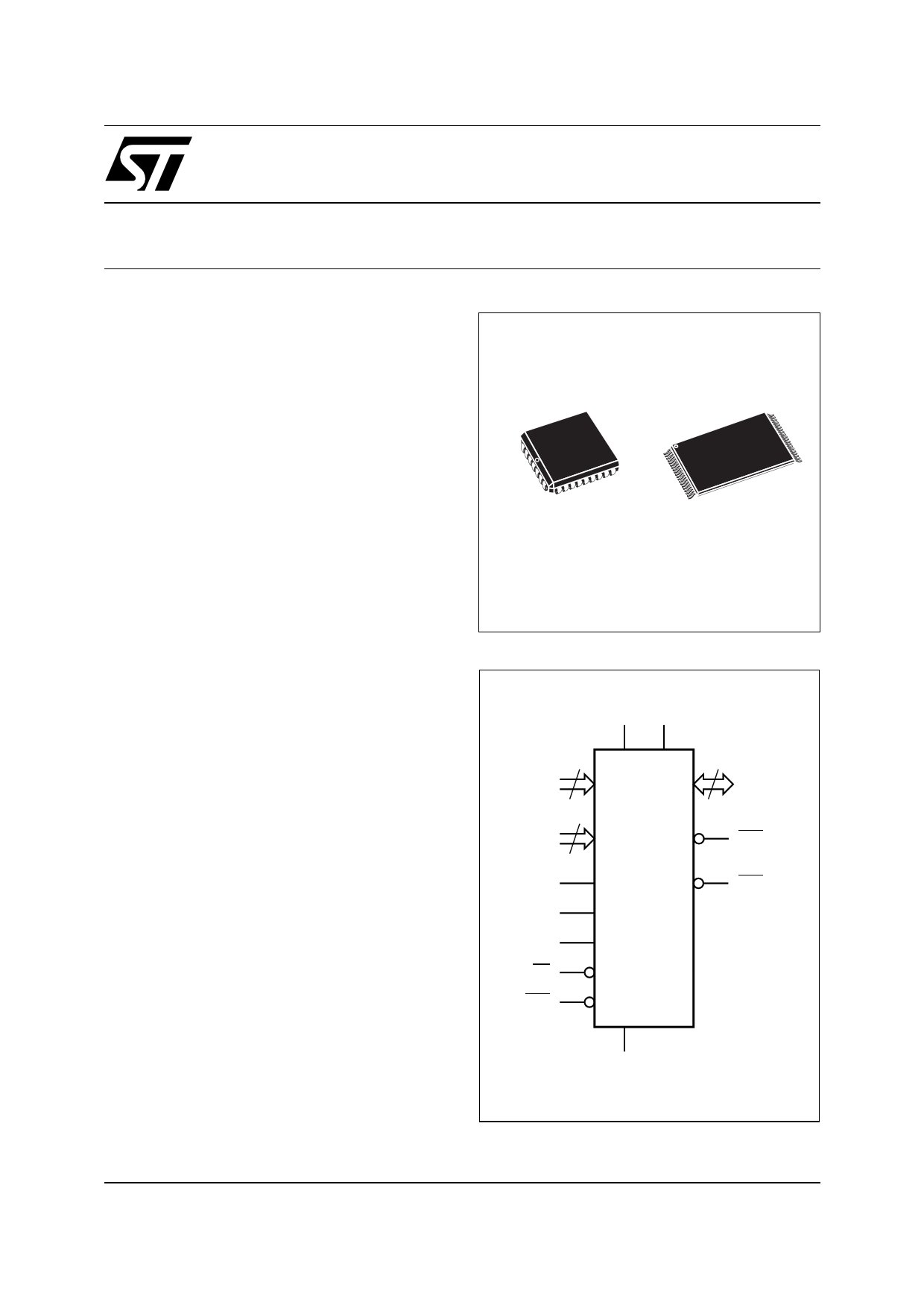
PLCC32 (K)
TSOP40 (N)
10 x 20mm
Figure 1. Logic Diagram (FWH Interface)
VCC VPP
ID0-ID3
FGPI0-
FGPI4
4
5
FWH4
CLK
IC
RP
INIT
M50FW040
4
FWH0-
FWH3
WP
TBL
VSS
AI03623
March 2002
1/32
1 page 
M50FW040
Table 3. Absolute Maximum Ratings (1)
Symbol
Parameter
Value
Unit
Ambient Operating Temperature (Temperature Range Option 1)
0 to 70
TA
Ambient Operating Temperature (Temperature Range Option 5)
–20 to 85
°C
°C
TBIAS
Temperature Under Bias
–50 to 125
°C
TSTG
Storage Temperature
–65 to 150
°C
VIO (2)
Input or Output Voltage
–0.6 to VCC + 0.6
V
VCC Supply Voltage
–0.6 to 4
V
VPP Program Voltage
–0.6 to 13
V
Note: 1. Except for the rating "Operating Temperature Range", stresses above those listed in the Table "Absolute Maximum Ratings" may
cause permanent damage to the device. These are stress ratings only and operation of the device at these or any other conditions
above those indicated in the Operating sections of this specification is not implied. Exposure to Absolute Maximum Rating condi-
tions for extended periods may affect device reliability. Refer also to the STMicroelectronics SURE Program and other relevant qual-
ity documents.
2. Minimum Voltage may undershoot to –2V and for less than 20ns during transitions. Maximum Voltage may overshoot to VCC + 2V
and for less than 20ns during transitions.
Protect, WP, does not affect the protection of the
Top Block (Block 7).
Write Protect, WP, must be set prior to a Program
or Erase operation is initiated and must not be
changed until the operation completes or unpre-
dictable results may occur. Care should be taken
to avoid unpredictable behavior by changing WP
during Program or Erase Suspend.
Reserved for Future Use (RFU). These pins do
not have assigned functions in this revision of the
part. They must be left disconnected.
Address/Address Multiplexed (A/A Mux)
Signal Descriptions
For the Address/Address Multiplexed (A/A Mux)
Interface see Figure 2, Logic Diagram, and Table
2, Signal Names.
Address Inputs (A0-A10). The Address Inputs
are used to set the Row Address bits (A0-A10) and
the Column Address bits (A11-A18). They are
latched during any bus operation by the Row/Col-
umn Address Select input, RC.
Data Inputs/Outputs (DQ0-DQ7). The Data In-
puts/Outputs hold the data that is written to or read
from the memory. They output the data stored at
the selected address during a Bus Read opera-
tion. During Bus Write operations they represent
the commands sent to the Command Interface of
the internal state machine. The Data Inputs/Out-
puts, DQ0-DQ7, are latched during a Bus Write
operation.
Output Enable (G). The Output Enable, G, con-
trols the Bus Read operation of the memory.
Write Enable (W). The Write Enable, W, controls
the Bus Write operation of the memory’s Com-
mand Interface.
Row/Column Address Select (RC). The Row/
Column Address Select input selects whether the
Address Inputs should be latched into the Row Ad-
dress bits (A0-A10) or the Column Address bits
(A11-A18). The Row Address bits are latched on
the falling edge of RC whereas the Column Ad-
dress bits are latched on the rising edge.
Ready/Busy Output (RB). The Ready/Busy pin
gives the status of the memory’s Program/Erase
Controller. When Ready/Busy is Low, VOL, the
memory is busy with a Program or Erase operation
and it will not accept any additional Program or
Erase command except the Program/Erase Sus-
pend command. When Ready/Busy is High, VOH,
the memory is ready for any Read, Program or
Erase operation.
Supply Signal Descriptions
The Supply Signals are the same for both interfac-
es.
VCC Supply Voltage. The VCC Supply Voltage
supplies the power for all operations (Read, Pro-
gram, Erase etc.).
The Command Interface is disabled when the VCC
Supply Voltage is less than the Lockout Voltage,
VLKO. This prevents Bus Write operations from ac-
cidentally damaging the data during power up,
power down and power surges. If the Program/
Erase Controller is programming or erasing during
this time then the operation aborts and the memo-
ry contents being altered will be invalid. After VCC
becomes valid the Command Interface is reset to
Read mode.
A 0.1µF capacitor should be connected between
the VCC Supply Voltage pins and the VSS Ground
pin to decouple the current surges from the power
supply. Both VCC Supply Voltage pins must be
connected to the power supply. The PCB track
widths must be sufficient to carry the currents re-
quired during program and erase operations.
VPP Optional Supply Voltage. The VPP Optional
Supply Voltage pin is used to select the Fast Erase
5/32
5 Page 
M50FW040
Table 10. Commands
Bus Write Operations
Command
1st
2nd
Address
Data
Address
Data
Read Memory Array
1X
FFh
Read Status Register
1X
70h
Read Electronic Signature
1
1
X
X
90h
98h
Program
2X
2X
40h PA
10h PA
PD
PD
Erase
2X
20h BA D0h
Clear Status Register
1X
50h
Program/Erase Suspend
1
X
B0h
Program/Erase Resume
1
X
D0h
1X
00h
1X
01h
Invalid/Reserved
1X
60h
1X
2Fh
1X
C0h
Note: X Don’t Care, PA Program Address, PD Program Data, BA Any address in the Block.
Read Memory Array. After a Read Memory Array command, read the memory as normal until another command is issued.
Read Status Register. After a Read Status Register command, read the Status Register as normal until another command is issued.
Read Electronic Signature. After a Read Electronic Signature command, read Manufacturer Code, Device Code until another com-
mand is issued.
Erase, Program. After these commands read the Status Register until the command completes and another command is issued.
Clear Status Register. After the Clear Status Register command bits 1, 3, 4 and 5 in the Status Register are reset to ‘0’.
Program/Erase Suspend. After the Program/Erase Suspend command has been accepted, issue Read Memory Array, Read Status
Register, Program (during Erase suspend) and Program/Erase resume commands.
Program/Erase Resume. After the Program/Erase Resume command the suspended Program/Erase operation resumes, read the
Status Register until the Program/Erase Controller completes and the memory returns to Read Mode.
Invalid/Reserved. Do not use Invalid or Reserved commands.
Program/Erase Suspend Command. The Pro-
gram/Erase Suspend command can be used to
pause a Program or Erase operation. One Bus
Write cycle is required to issue the Program/Erase
Suspend command and pause the Program/Erase
Controller. Once the command is issued it is nec-
essary to poll the Program/Erase Controller Status
bit to find out when the Program/Erase Controller
has paused; no other commands will be accepted
until the Program/Erase Controller has paused.
After the Program/Erase Controller has paused,
the memory will continue to output the Status Reg-
ister until another command is issued.
During the polling period between issuing the Pro-
gram/Erase Suspend command and the Program/
Erase Controller pausing it is possible for the op-
eration to complete. Once Program/Erase Control-
ler Status bit indicates that the Program/Erase
Controller is no longer active, the Program Sus-
pend Status bit or the Erase Suspend Status bit
can be used to determine if the operation has com-
pleted or is suspended. For timing on the delay be-
tween issuing the Program/Erase Suspend
command and the Program/Erase Controller
pausing see Table 11.
During Program/Erase Suspend the Read Memo-
ry Array, Read Status Register, Read Electronic
Signature and Program/Erase Resume com-
mands will be accepted by the Command Inter-
face. Additionally, if the suspended operation was
Erase then the Program command will also be ac-
cepted; only the blocks not being erased may be
read or programmed correctly.
See Figures 15, Program Suspend & Resume
Flowchart and Pseudo Code, and 17, Erase Sus-
pend & Resume Flowchart and Pseudo Code, for
suggested flowcharts on using the Program/Erase
Suspend command.
Program/Erase Resume Command. The Pro-
gram/Erase Resume command can be used to re-
start the Program/Erase Controller after a
Program/Erase Suspend operation has paused it.
One Bus Write cycle is required to issue the Pro-
gram/Erase Resume command. Once the com-
mand is issued subsequent Bus Read operations
read the Status Register.
11/32
11 Page | ||
| Páginas | Total 30 Páginas | |
| PDF Descargar | [ Datasheet M50FW040.PDF ] | |
Hoja de datos destacado
| Número de pieza | Descripción | Fabricantes |
| M50FW040 | "4 Mbit 512Kb x8 | Uniform Block 3V Supply Firmware Hub Flash Memory" |
| M50FW040 | 4 Mbit 512Kb x8/ Uniform Block 3V Supply Firmware Hub Flash Memory | ST Microelectronics |
| Número de pieza | Descripción | Fabricantes |
| SLA6805M | High Voltage 3 phase Motor Driver IC. |
Sanken |
| SDC1742 | 12- and 14-Bit Hybrid Synchro / Resolver-to-Digital Converters. |
Analog Devices |
|
DataSheet.es es una pagina web que funciona como un repositorio de manuales o hoja de datos de muchos de los productos más populares, |
| DataSheet.es | 2020 | Privacy Policy | Contacto | Buscar |