|
|
|
PDF M50FW002 Data sheet ( Hoja de datos )
| Número de pieza | M50FW002 | |
| Descripción | 2 Mbit 256Kb x8/ Boot Block 3V Supply Firmware Hub Flash Memory | |
| Fabricantes | ST Microelectronics | |
| Logotipo | ||
Hay una vista previa y un enlace de descarga de M50FW002 (archivo pdf) en la parte inferior de esta página. Total 30 Páginas | ||
|
No Preview Available !
M50FW002
2 Mbit (256Kb x8, Boot Block)
3V Supply Firmware Hub Flash Memory
PRELIMINARY DATA
FEATURES SUMMARY
s SUPPLY VOLTAGE
– VCC = 3 V to 3.6 V for Program, Erase and
Read Operations
– VPP = 12 V for Fast Program and Fast Erase
(optional)
s TWO INTERFACES
– Firmware Hub (FWH) Interface for embedded
operation with PC Chipsets
– Address/Address Multiplexed (A/A Mux)
Interface for programming equipment
compatibility
s FIRMWARE HUB (FWH) HARDWARE
INTERFACE MODE
– 5 Signal Communication Interface supporting
Read and Write Operations
– Hardware Write Protect Pins for Block
Protection
– Register Based Read and Write Protection
– 5 Additional General Purpose Inputs for
platform design flexibility
– Synchronized with 33MHz PCI clock
– Multi-byte Read Operation (1-byte, 16-byte,
32-byte)
s PROGRAMMING TIME
– 10 µs typical
– Quadruple Byte Programming Option
s 7 MEMORY BLOCKS
– 1 Boot Block (Top Location)
– 4 Main Blocks and 2 Parameter Blocks
s PROGRAM/ERASE CONTROLLER
– Embedded Byte Program, Block Erase and
Chip Erase algorithms
– Status Register Bits
s PROGRAM and ERASE SUSPEND
s FOR USE in PC BIOS APPLICATIONS
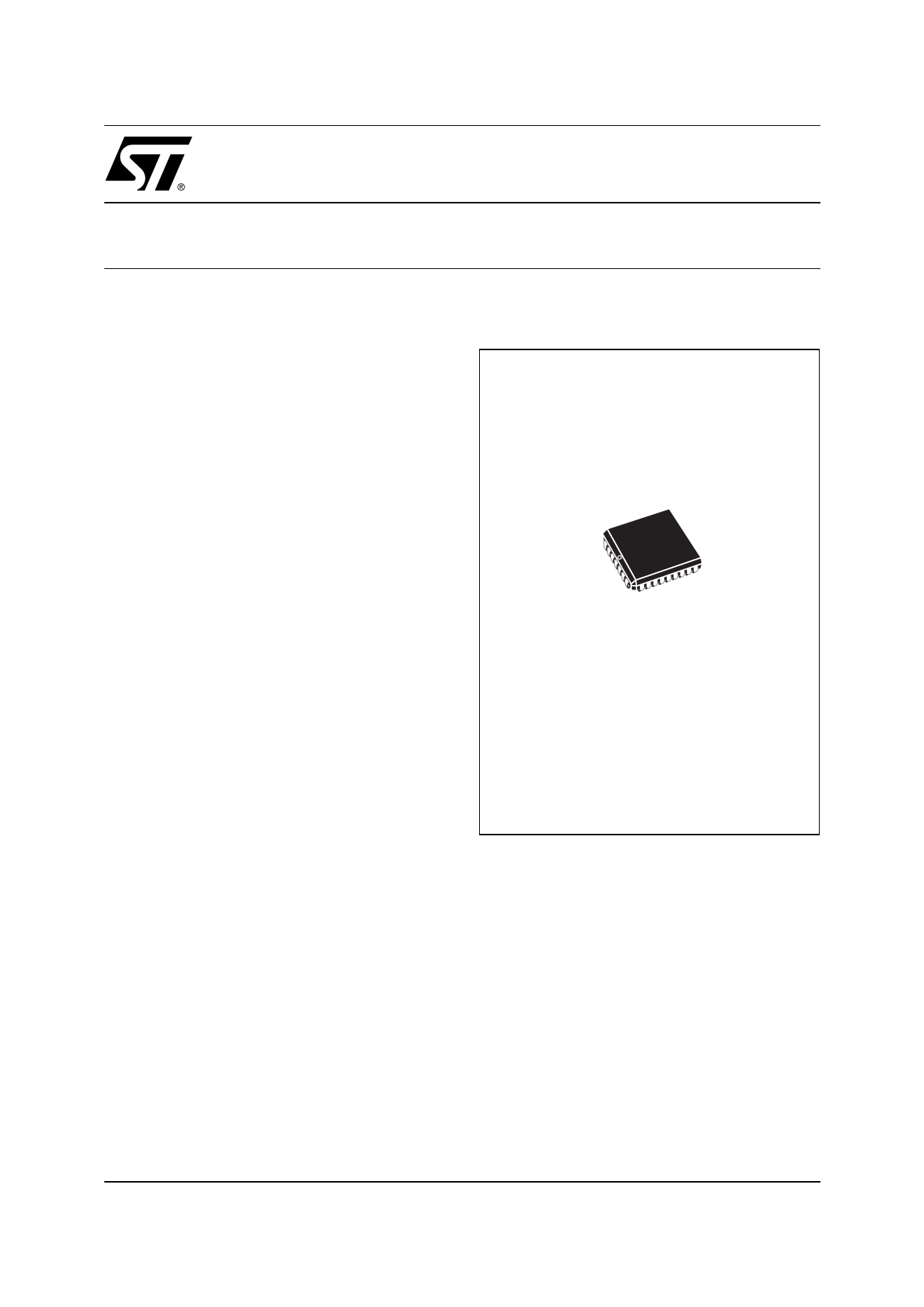
Figure 1. Packages
PLCC32 (K)
s ELECTRONIC SIGNATURE
– Manufacturer Code: 20h
– Device Code: 29h
May 2002
This is preliminary information on a new product now in development or undergoing evaluation. Details are subject to change without notice.
1/39
1 page 
Figure 3. Logic Diagram (FWH Interface)
VCC VPP
4
ID0-ID3
FGPI0-
FGPI4
5
FWH4
CLK
IC
RP
INIT
M50FW002
4
FWH0-
FWH3
WP
TBL
VSS
AI05747
Table 1. Signal Names (FWH Interface)
FWH0-FWH3 Input/Output Communications
FWH4
Input Communication Frame
ID0-ID3
Identification Inputs
FGPI0-FGPI4 General Purpose Inputs
IC Interface Configuration
RP Interface Reset
INIT CPU Reset
CLK
Clock
TBL Top Block Lock
WP Write Protect
RFU
Reserved for Future Use. Leave
disconnected
VCC Supply Voltage
VPP
Optional Supply Voltage for Fast
Erase Operations
VSS Ground
NC Not Connected Internally
M50FW002
Figure 4. Logic Diagram (A/A Mux Interface)
VCC VPP
11
A0-A10
8
DQ0-DQ7
RC
M50FW002
IC RB
G
W
RP
VSS
AI05748
Table 2. Signal Names (A/A Mux Interface)
IC Interface Configuration
A0-A10
Address Inputs
DQ0-DQ7
Data Inputs/Outputs
G Output Enable
W Write Enable
RC Row/Column Address Select
RB Ready/Busy Output
RP Interface Reset
VCC Supply Voltage
VPP
Optional Supply Voltage for Fast
Program and Fast Erase Operations
VSS Ground
NC Not Connected Internally
5/39
5 Page 
M50FW002
Address/Address Multiplexed (A/A Mux) Bus
Operations
The Address/Address Multiplexed (A/A Mux)
Interface has a more traditional style interface.
The signals consist of a multiplexed address
signals (A0-A10), data signals, (DQ0-DQ7) and
three control signals (RC, G, W). An additional
signal, RP, can be used to reset the memory.
The Address/Address Multiplexed (A/A Mux)
Interface is included for use by Flash
Programming equipment for faster factory
programming. Only a subset of the features
available to the Firmware Hub (FWH) Interface are
available; these include all the Commands but
exclude the Security features and other registers.
The following operations can be performed using
the appropriate bus cycles: Bus Read, Bus Write,
Output Disable and Reset.
When the Address/Address Multiplexed (A/A Mux)
Interface is selected all the blocks are
unprotected. It is not possible to protect any blocks
through this interface.
Bus Read. Bus Read operations are used to
output the contents of the Memory Array, the
Electronic Signature and the Status Register. A
valid Bus Read operation begins by latching the
Row Address and Column Address signals into
the memory using the Address Inputs, A0-A10,
and the Row/Column Address Select RC. Then
Write Enable (W) and Interface Reset (RP) must
be High, VIH, and Output Enable, G, Low, VIL, in
Table 6. A/A Mux Bus Operations
Operation
GW
Bus Read
VIL VIH
Bus Write
VIH VIL
Output Disable
VIH VIH
Reset
VIL or VIH
VIL or VIH
order to perform a Bus Read operation. The Data
Inputs/Outputs will output the value, see Figure
12, Read AC Waveforms (A/A Mux Interface), and
Table 24, A/A Mux Interface Read AC
Characteristics, for details of when the output
becomes valid.
Bus Write. Bus Write operations write to the
Command Interface. A valid Bus Write operation
begins by latching the Row Address and Column
Address signals into the memory using the
Address Inputs, A0-A10, and the Row/Column
Address Select RC. The data should be set up on
the Data Inputs/Outputs; Output Enable, G, and
Interface Reset, RP, must be High, VIH and Write
Enable, W, must be Low, VIL. The Data Inputs/
Outputs are latched on the rising edge of Write
Enable, W. See Figure 13, and Table 25, A/A Mux
Interface Write AC Characteristics, for details of
the timing requirements.
Output Disable. The data outputs are high-im-
pedance when the Output Enable, G, is at VIH.
Reset. During Reset mode all internal circuits are
switched off, the memory is deselected and the
outputs are put in high-impedance. The memory is
in Reset mode when RP is Low, VIL. RP must be
held Low, VIL for tPLPH. If RP is goes Low, VIL,
during a Program or Erase operation, the
operation is aborted and the memory cells affected
no longer contain valid data; the memory can take
up to tPLRH to abort a Program or Erase operation.
RP VPP DQ7-DQ0
VIH
Don’t Care
Data Output
VIH VCC or VPPH Data Input
VIH Don’t Care
Hi-Z
VIL Don’t Care
Hi-Z
Table 7. Manufacturer and Device Codes
Operation
GW
Manufacturer Code
VIL
VIH
Device Code
VIL VIH
RP A17-A1 A0 DQ7-DQ0
VIH VIL VIL 20h
VIH VIL VIH 29h
11/39
11 Page | ||
| Páginas | Total 30 Páginas | |
| PDF Descargar | [ Datasheet M50FW002.PDF ] | |
Hoja de datos destacado
| Número de pieza | Descripción | Fabricantes |
| M50FW002 | "2 Mbit 256Kb x8 | Boot Block 3V Supply Firmware Hub Flash Memory" |
| M50FW002 | 2 Mbit 256Kb x8/ Boot Block 3V Supply Firmware Hub Flash Memory | ST Microelectronics |
| Número de pieza | Descripción | Fabricantes |
| SLA6805M | High Voltage 3 phase Motor Driver IC. |
Sanken |
| SDC1742 | 12- and 14-Bit Hybrid Synchro / Resolver-to-Digital Converters. |
Analog Devices |
|
DataSheet.es es una pagina web que funciona como un repositorio de manuales o hoja de datos de muchos de los productos más populares, |
| DataSheet.es | 2020 | Privacy Policy | Contacto | Buscar |