|
|
|
PDF M52760SP Data sheet ( Hoja de datos )
| Número de pieza | M52760SP | |
| Descripción | PLL-SPLIT VIF/SIF IC | |
| Fabricantes | Mitsubishi | |
| Logotipo | ||
Hay una vista previa y un enlace de descarga de M52760SP (archivo pdf) en la parte inferior de esta página. Total 8 Páginas | ||
|
No Preview Available !
MITSUBISHI ICs (TV)
M52760SP
PLL-SPLIT VIF/SIF IC
DESCRIPTION
The M52760SP is IF signal-processing IC for VCRs and TVs. It
enable the PLL detection system despite size as small as that of
conventional quasi-synchronous VIF/SIF detector, IF/RF AGC, SIF
limiter, FM detector and EQ AMP.
FEATURES
• Video detection output is 2VP-P. It has built-in EQ AMP.
• The package is a 20-pin shrink-DIP, suitable for space saving.
• The video detector uses PLL for full synchronous detection
circuit. It produces excellent characteristics of DG, DP, 920kHz
beat, and cross color.
• Dynamic AGC realizes high speed response with only single
filter.
• Video IF and sound IF signal processings are separated from
each other. VCO output is used to obtain intercarrier.
This PLL-SPLIT method provide good sound sensitivity and
reduces buzz.
• As AFT output voltage uses the APC output voltage, VCO coil is
not used.
• Audio FM demodulation uses PLL system, so it has wide
frequency range with no external parts and no adjustment.
• QIF AMP has a fixed gain, and good characteristic for NICAM.
APPLICATION
TV sets, VCR tuners
RECOMMENDED OPERATING CONDITION
In case of Vcc and Vreg. out short
Supply voltage range....................................................4.75 to 5.25V
Recommended supply voltage...................................................5.0V
In case of Vreg. out open
Supply voltage range......................................................8.5 to 12.5V
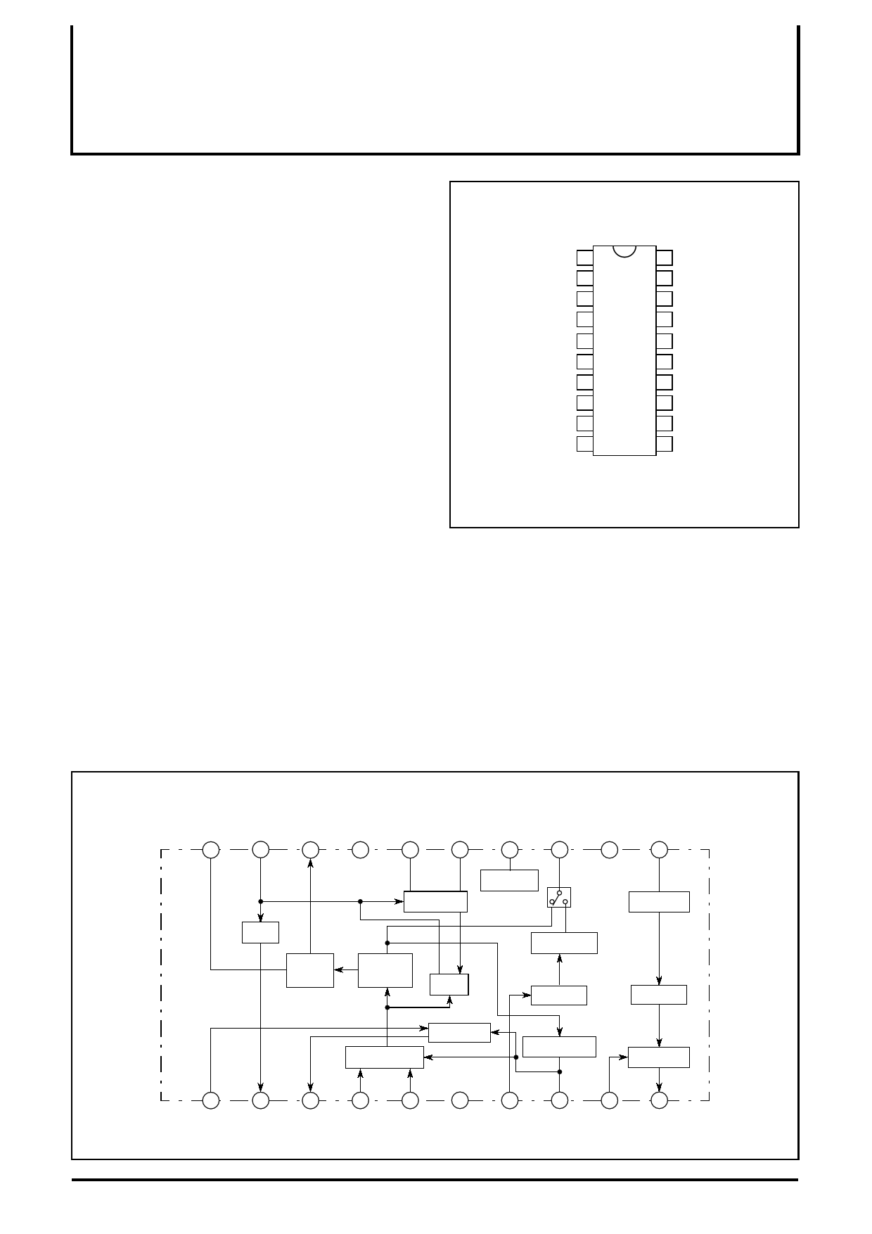
PIN CONFIGURATION (TOP VIEW)
RF AGC DELAY 1
AFT OUT 2
RF AGC OUT 3
VIF IN 4
VIF IN 5
GND 6
QIF DET IN 7
IF AGC FILTER 8
NFB 9
AUDIO OUT 10
20 EQ F/B
19 APC FILTER
18 VIDEO OUT
17 Vreg. OUT
16 VCO COIL
15 VCO COIL
14 Vcc
13 QIF OUT
12 AFT SW/NPSW
11 LIMITER IN
Outline 20P4B
BLOCK DIAGRAM
APC FILTER
Vreg. OUT
VCO COIL
EQ F/B
VIDEO OUT
VCO COIL
20 19 18 17 16 15
Vcc
14
QIF OUT
LIMITER IN
AFT SW/NPSW
13 12 11
VCO
Vcc REG
Inter
Split
LIM AMP
AFT
EQ
AMP
VIDEO
DET
APC
QIF DET
QIF AMP
FM DET
VIF AMP
RF AGC
IF AGC
AF AMP
1234
RF AGC DELAY
RF AGC OUT
AFT OUT
VIF IN
5
VIF IN
6
GND
789
QIF DET IN
NFB
IF AGC FILTER
10
AUDIO OUT
1
1 page 
MITSUBISHI ICs (TV)
M52760SP
PLL-SPLIT VIF/SIF IC
µ AFT sensitivity, V2H Maximum AFT voltage, V2L Minimum AFT
voltage
1. Input SG10 into VIF IN , and set the frequency of SG10 so that
the voltage of AFT output TP2 is 3V. This frequency is f (3).
2. Set the frequency of SG10 so that the AFT output voltage is 2V.
This frequency is f (2)
3. IN the graph, maximum and minimum DC voltage are V2H and
V2L, respectively.
TP2
Voltage
3V
V2H
2V
V2L
f (3) f (2) f (MHz)
1000 (mV)
µ = (mV/kHz)
f (2) - f (3) (kHz)
IM Intermodulation
1. Input SG11 into VIF IN, and measure EQ output TP18A with an
oscilloscope.
2. Adjust AGC filter voltage V8 so that the minimum DC level of the
output waveform is 1.0V.
3. At this time, measure, TP18A with a spectrum analyzer.
The intermodulation is defined as a difference between 1.07MHz
and 4.43MHz frequency components.
LIM Limiting sensitivity
1. Input SG17 (SG21) into SIF input, and measure the 400Hz
component level of AF output TP10.
2. Input SG19 (SG23) into SIF input, and measure the 400Hz
component level of AF output TP10.
3. The input limiting sensitivity is defined as the input level when a
difference between each 400Hz components of audio output
(TP10) is 30dB, as shown below.
Audio output
(mVrms)
30dB
Audio output while
SG17 (SG21) is input
Audio output while
SG19 (SG23) is input
AMR AM Rejection
1. Input SG18 into SIF input, and measure the output level of AF
output TP10. This level is VAM.
2. AMR is;
VoAF (mVr.m.s)
AMR=20log
(dB)
VAM (mVr.m.s)
AF S/N
1. Input SG19 into SIF input, and measure the output noise level of
AF output TP1. This level is VN.
2. S/N is;
VoAF (mVr.m.s)
S/N=20log VN (mVr.m.s) (dB)
CQIF QIF control
Lower the voltage of V7, and measure the voltage of V7 when the
DC voltage of TP13 begins to change.
THE NOTE IN THE SYSTEM SETUP
M52760SP has 2 power supply pins of Vcc (pin 14) and Vreg.OUT
(pin 17) .
Pin 14 is for AFT output, RF AGC output circuits and 5V regulated
power supply circuit and Pin 17 is for the other circuit blocks.
In case M52760SP is used together with other ICs like VIF
operating at more than 5V, the same supply voltage as that of
connected ICs is applied to VCC and Vreg.Out is opened. The other
circuit blocks, connected to Vreg.OUT are powered by internal 5V
regulated power supply.
In case the connecting ICs are operated at 5V, 5V is supplied to
both VCC and Vreg.OUT.
LOGIC TABLE
10k “H”
10k “L”
20k “H”
20k “L”
20k “H”
20k “L”
AF
NTSC
PAL
AFT
DEFEAT
NORMAL
DEFEAT
NORMAL
(dBµ) SIF input
5
5 Page | ||
| Páginas | Total 8 Páginas | |
| PDF Descargar | [ Datasheet M52760SP.PDF ] | |
Hoja de datos destacado
| Número de pieza | Descripción | Fabricantes |
| M52760SP | PLL-SPLIT VIF/SIF IC | Mitsubishi |
| M52760SP | PLL-SPLIT VIF/SIF IC | Mitsubishi |
| Número de pieza | Descripción | Fabricantes |
| SLA6805M | High Voltage 3 phase Motor Driver IC. |
Sanken |
| SDC1742 | 12- and 14-Bit Hybrid Synchro / Resolver-to-Digital Converters. |
Analog Devices |
|
DataSheet.es es una pagina web que funciona como un repositorio de manuales o hoja de datos de muchos de los productos más populares, |
| DataSheet.es | 2020 | Privacy Policy | Contacto | Buscar |