|
|
|
PDF IDT74FCT237ATPB Data sheet ( Hoja de datos )
| Número de pieza | IDT74FCT237ATPB | |
| Descripción | FAST CMOS OCTAL TRANSPARENT LATCHES | |
| Fabricantes | Integrated Device Tech | |
| Logotipo | ||
Hay una vista previa y un enlace de descarga de IDT74FCT237ATPB (archivo pdf) en la parte inferior de esta página. Total 8 Páginas | ||
|
No Preview Available !
Integrated Device Technology, Inc.
FAST CMOS OCTAL
TRANSPARENT
LATCHES
IDT54/74FCT373T/AT/CT/DT - 2373T/AT/CT
IDT54/74FCT533T/AT/CT
IDT54/74FCT573T/AT/CT/DT - 2573T/AT/CT
FEATURES:
– Reduced system switching noise
• Common features:
– Low input and output leakage ≤1µA (max.)
– CMOS power levels
– True TTL input and output compatibility
– VOH = 3.3V (typ.)
– VOL = 0.3V (typ.)
– Meets or exceeds JEDEC standard 18 specifications
– Product available in Radiation Tolerant and Radiation
Enhanced versions
– Military product compliant to MIL-STD-883, Class B
and DESC listed (dual marked)
– Available in DIP, SOIC, SSOP, QSOP, CERPACK
and LCC packages
• Features for FCT373T/FCT533T/FCT573T:
– Std., A, C and D speed grades
– High drive outputs (-15mA IOH, 48mA IOL)
– Power off disable outputs permit “live insertion”
• Features for FCT2373T/FCT2573T:
– Std., A and C speed grades
– Resistor output (-15mA IOH, 12mA IOL Com.)
(-12mA IOH, 12mA IOL Mil.)
DESCRIPTION:
The FCT373T/FCT2373T, FCT533T and FCT573T/
FCT2573T are octal transparent latches built using an ad-
vanced dual metal CMOS technology. These octal latches
have 3-state outputs and are intended for bus oriented appli-
cations. The flip-flops appear transparent to the data when
Latch Enable (LE) is HIGH. When LE is LOW, the data that
meets the set-up time is latched. Data appears on the bus
when the Output Enable (OE) is LOW. When OE is HIGH, the
bus output is in the high- impedance state.
The FCT2373T and FCT2573T have balanced drive out-
puts with current limiting resistors. This offers low ground
bounce, minimal undershoot and controlled output fall times-
reducing the need for external series terminating resistors.
The FCT2xxxT parts are plug-in replacements for FCTxxxT
parts.
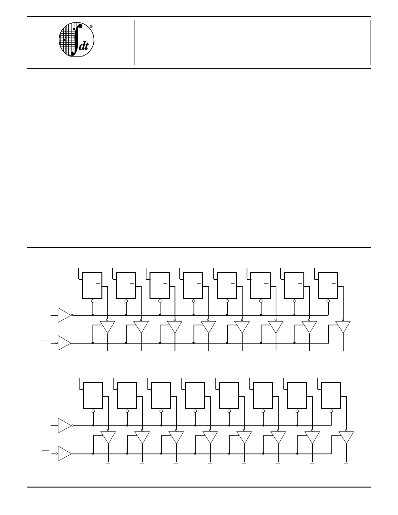
FUNCTIONAL BLOCK DIAGRAM IDT54/74FCT373T/2373T AND IDT54/74FCT573T/2573T
D0 D1 D2 D3 D4 D5 D6 D7
D
O
G
D
O
G
D
O
G
D
O
G
D
O
G
D
O
G
D
O
G
D
O
G
LE
OE
O0 O1 O2 O3
FUNCTIONAL BLOCK DIAGRAM IDT54/74FCT533T
D0 D1 D2 D3 D4
O4
D5
O5
D6
O6
D7
O7
2564 cnv* 01
D
O
G
D
O
G
D
O
G
D
O
G
D
O
G
D
O
G
D
O
G
D
O
G
LE
OE
O0 O1 O2 O3 O4 O5 O6 O7
The IDT logo is a registered trademark of Integrated Device Technology, Inc.
2564 cnv* 02
MILITARY AND COMMERCIAL TEMPERATURE RANGES
AUGUST 1995
©1995 Integrated Device Technology, Inc.
6.12
DSC-4216/6
1
1 page 
IDT54/74FCT373T/AT/CT/DT - 2373T/AT/CT, IDT54/74FCT533T/AT/CT, IDT54/74FCT573T/AT/CT/DT - 2573T/AT/CT
FAST CMOS OCTAL TRANSPARENT LATCHES
MILITARY AND COMMERCIAL TEMPERATURE RANGES
POWER SUPPLY CHARACTERISTICS
Symbol
∆ICC
ICCD
IC
Parameter
Quiescent Power Supply Current
TTL Inputs HIGH
Dynamic Power Supply
Current(4)
Total Power Supply Current(6)
Test Conditions(1)
VCC = Max.
VIN = 3.4V(3)
VCC = Max.
VIN = VCC FCTxxxT
Outputs Open
OE = GND
VIN = GND
FCT2xxxT
One Input Toggling
50% Duty Cycle
VCC = Max.
VIN = VCC FCTxxxT
Min. Typ.(2) Max.
— 0.5 2.0
— 0.15 0.25
— 0.06 0.12
— 1.5 3.5
Unit
mA
mA/
MHz
mA
Outputs Open
fi = 10MHz
50% Duty Cycle
OE = GND
LE = VCC
One Bit Toggling
VCC = Max.
VIN = GND FCT2xxxT —
VIN = 3.4 FCTxxxT
VIN = GND
FCT2xxxT
—
VIN = VCC FCTxxxT
—
0.6 2.2
1.8 4.5
0.9 3.2
3.0 6.0(5)
Outputs Open
VIN = GND FCT2xxxT —
1.2 3.4(5)
fi = 2.5MHz
50% Duty Cycle
OE = GND
VIN = 3.4 FCTxxxT — 5.0 14.0(5)
VIN = GND
LE = VCC
FCT2xxxT —
3.2 11.4(5)
Eight Bits Toggling
NOTES:
1. For conditions shown as Max. or Min., use appropriate value specified under Electrical Characteristics for the applicable device type.
2. Typical values are at VCC = 5.0V, +25°C ambient.
2564 tbl 09
3. Per TTL driven input (VIN = 3.4V). All other inputs at VCC or GND.
4. This parameter is not directly testable, but is derived for use in Total Power Supply Calculations.
5. Values for these conditions are examples of the ICC formula. These limits are guaranteed but not tested.
6. IC = IQUIESCENT + IINPUTS + IDYNAMIC
IC = ICC + ∆ICC DHNT + ICCD (fCP/2 + fiNi)
ICC = Quiescent Current
∆ICC = Power Supply Current for a TTL High Input (VIN = 3.4V)
DH = Duty Cycle for TTL Inputs High
NT = Number of TTL Inputs at DH
ICCD = Dynamic Current Caused by an Input Transition Pair (HLH or LHL)
fCP = Clock Frequency for Register Devices (Zero for Non-Register Devices)
fi = Input Frequency
Ni = Number of Inputs at fi
All currents are in milliamps and all frequencies are in megahertz.
6.12 5
5 Page | ||
| Páginas | Total 8 Páginas | |
| PDF Descargar | [ Datasheet IDT74FCT237ATPB.PDF ] | |
Hoja de datos destacado
| Número de pieza | Descripción | Fabricantes |
| IDT74FCT237ATP | FAST CMOS OCTAL TRANSPARENT LATCHES | Integrated Device Tech |
| IDT74FCT237ATPB | FAST CMOS OCTAL TRANSPARENT LATCHES | Integrated Device Tech |
| IDT74FCT237ATPY | FAST CMOS OCTAL TRANSPARENT LATCHES | Integrated Device Tech |
| IDT74FCT237ATPYB | FAST CMOS OCTAL TRANSPARENT LATCHES | Integrated Device Tech |
| Número de pieza | Descripción | Fabricantes |
| SLA6805M | High Voltage 3 phase Motor Driver IC. |
Sanken |
| SDC1742 | 12- and 14-Bit Hybrid Synchro / Resolver-to-Digital Converters. |
Analog Devices |
|
DataSheet.es es una pagina web que funciona como un repositorio de manuales o hoja de datos de muchos de los productos más populares, |
| DataSheet.es | 2020 | Privacy Policy | Contacto | Buscar |