|
|
PDF PCF8801U Data sheet ( Hoja de datos )
| Número de pieza | PCF8801U | |
| Descripción | LCD driver for 140 x 2 segments | |
| Fabricantes | NXP Semiconductors | |
| Logotipo | ||
Hay una vista previa y un enlace de descarga de PCF8801U (archivo pdf) en la parte inferior de esta página. Total 20 Páginas | ||
|
No Preview Available !
INTEGRATED CIRCUITS
DATA SHEET
PCF8801
LCD driver for 140 × 2 segments
Product specification
File under Integrated Circuits, IC12
2000 Feb 04
1 page 
Philips Semiconductors
LCD driver for 140 × 2 segments
Product specification
PCF8801
FUNCTIONAL DESCRIPTION
Refer to block diagram Fig.1. The PCF8801 comprises a
bi-directional 280-bit input shift register, 280-bit output
register, output multiplexer providing 140-segment outputs
via a routing block and output drivers, two 3-level
backplane outputs, internal oscillator and internal
power-on reset circuit. To reduce the length of routing
required between cascaded chips in multiple chip-on-glass
applications, all inputs/outputs for control lines, clock
signals and data are provided at both sides of the narrow
package.
Shift register
The 280-bit bi-directional shift register shifts data on the
rising edge of clock signal CLKI. The shift register output
bits are called SH1_1, SH1_2 to SH140_1, SH140_2.
The direction in which data is shifted and the pads that are
valid for inputs DI, CLKI and output CLKO, is determined
by the voltage level on pad DIR. The voltage on pad DIR
must be tied to either VDD or VSS and must not be switched
when the PCF8801 is operating. The relationship between
the status of pad DIR and the other pads connected to the
shift register is shown in Table 1.
Table 1 280-bit bi-directional shift register pads
SHIFT DIRECTION
Data input DI(1)
Data output DO(2)
Clock input CLKI
Clock output CLKO(2)
First bit shifted
Last bit shifted(3)
VALID PAD
DIR = 1
DIR = 0
DI1
DO1 and DO2
CLK1
CLK2
SH140_2
SH1_1
DI2
DO1 and DO2
CLK2
CLK1
SH1_1
SH140_2
Notes
1. The invalid DI pad must be connected to either VDD or
VSS.
2. Pads DO and CLKO are used when PCF8801 devices
are connected in cascade.
3. The last bit is loaded into a flip-flop whose output is
connected to pad DO. The value of the last bit appears
at pad DO delayed by a 1⁄2 CLKI period.
Output register
The 280-data bits (SH1_1, SH1_2 to SH140_1, SH140_2)
from the output of the shift register are transferred to the
input of the 280 bit output register. Data is transferred
when either pad LDPI goes HIGH or when pad LDNI goes
LOW. The output register bits are called IO1_1, IO1_2
to IO140_1, IO140_2. The pads that are valid for
inputs LDPI, LDNI, OSCI, and outputs LDPO, LDNO,
OSCO are determined by the voltage level on pad DIR.
During a positive pulse on pad LDPI, pad LDNI must stay
HIGH, or during a negative pulse on pad LDNI, pad LDPI
must stay LOW. The voltage on pad DIR must be tied to
either VDD or VSS and must not be switched when the
PCF8801 is operating. The relationship between the
status of pad DIR and the other pads connected to the
output register is shown in Table 2.
Table 2 280-bit output register pads
SHIFT DIRECTION
Data load input LDPI
Data load output LDPO
Data load input LDNI
Data load output LDNO
Multiplexing clock input OSCI
Multiplexing clock output OSCO
VALID PAD
DIR = 1 DIR = 0
LDP1
LDP2
LDN1
LDN2
OSC1
OSC2
LDP2
LDP1
LDN2
LDN1
OSC2
OSC1
Output multiplexer, frame generator and backplane
drivers
The 280 data bits (IO1_1, IO1_2 to IO140_1, IO140_2)
from the output register are transferred to the input of the
output multiplexer which multiplexes the data at the rate of
1 : 2. The 140 output bits from the output multiplexer are
called OM1 to OM140. The frame generator outputs two
control signals derived from the LCD multiplex clock
(OSCI) called COMMON (1⁄2 fOSC) and M (1⁄4 fOSC) which
control the output multiplexer and the backplane drivers.
The operation of the output multiplexer is defined in
Table 3.
2000 Feb 04
5
5 Page 
Philips Semiconductors
LCD driver for 140 × 2 segments
Product specification
PCF8801
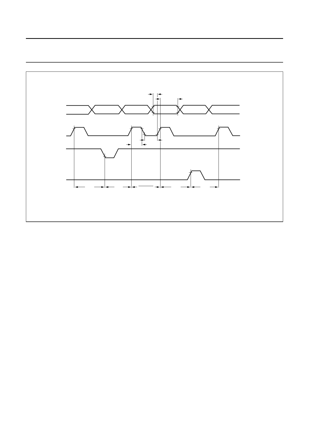
handbook, full pagewidth
DI
CLK
LDN
LDP
tsu(DI-CLK)
th(D)
tH(CLK)(LD)
tL(CLK)(LD)
tsep
1
tsep fclk(CLK)
tsep
tsep
MGL919
Fig.5 Serial interface timing.
2000 Feb 04
11
11 Page | ||
| Páginas | Total 20 Páginas | |
| PDF Descargar | [ Datasheet PCF8801U.PDF ] | |
Hoja de datos destacado
| Número de pieza | Descripción | Fabricantes |
| PCF8801 | LCD driver for 140 x 2 segments | NXP Semiconductors |
| PCF8801U | LCD driver for 140 x 2 segments | NXP Semiconductors |
| Número de pieza | Descripción | Fabricantes |
| SLA6805M | High Voltage 3 phase Motor Driver IC. |
Sanken |
| SDC1742 | 12- and 14-Bit Hybrid Synchro / Resolver-to-Digital Converters. |
Analog Devices |
|
DataSheet.es es una pagina web que funciona como un repositorio de manuales o hoja de datos de muchos de los productos más populares, |
| DataSheet.es | 2020 | Privacy Policy | Contacto | Buscar |
