|
|
PDF UPD16732AN Data sheet ( Hoja de datos )
| Número de pieza | UPD16732AN | |
| Descripción | 384-OUTPUT TFT-LCD SOURCE DRIVER COMPATIBLE WITH 64-GRAY SCALES | |
| Fabricantes | NEC | |
| Logotipo |  |
|
Hay una vista previa y un enlace de descarga de UPD16732AN (archivo pdf) en la parte inferior de esta página. Total 24 Páginas | ||
|
No Preview Available !
DATA SHEET
MOS INTEGRATED CIRCUIT
µ PD16732A, 16732B
384-OUTPUT TFT-LCD SOURCE DRIVER
(COMPATIBLE WITH 64-GRAY SCALES)
DESCRIPTION
The µ PD16732A, 16732B are a source driver for TFT-LCDs capable of dealing with displays with 64-gray scales.
Data input is based on digital input configured as 6 bits by 6 dots (2 pixels), which can realize a full-color display of
260,000 colors by output of 64 values γ -corrected by an internal D/A converter and 5-by-2 external power modules.
Because the output dynamic range is as large as VSS2 + 0.1 V to VDD2 – 0.1 V, level inversion operation of the LCD’s
common electrode is rendered unnecessary. Also, to be able to deal with dot-line inversion, n-line inversion and
column line inversion when mounted on a single side, this source driver is equipped with a built-in 6-bit D/A converter
circuit whose odd output pins and even output pins respectively output gray scale voltages of differing polarity.
Assuring a maximum clock frequency of 65 MHz when driving at 3.0 V, 45 MHz when driving at 2.3 V, this driver is
applicable to XGA-standard TFT-LCD panels and SXGA TFT-LCD panels by input display signal 2 systems (Clock
divide).
FEATURES
• CMOS level input (2.3 V to 3.6 V)
• 384 Outputs
• Input of 6 bits (gradation data) by 6 dots
• Capable of outputting 64 values by means of 5-by-2 external power modules (10 units) and
a D/A converter (R-DAC)
• High-speed data transfer: fMAX. = 65 MHz (internal data transfer speed when operating at VDD1 = 3.0 V)
• Output dynamic range VSS2 + 0.1 V to VDD2 – 0.1 V
• Apply for dot-line inversion, n-line inversion and column line inversion
• Output Voltage polarity inversion function (POL)
• Display data inversion function (POL2)
• Low power control function (LPC)
• Logic power supply voltage (VDD1) : 2.3 V to 3.6 V
• Driver power supply voltage (VDD2) : 8.5 ± 0.5 V
• Different point between µ PD16732A, 16732B : The ladder resistors value(Refer to 5. RELATIONSHIP
BETWEEN INPUT DATA AND OUTPUT VOLTAGE VALUE)
ORDERING INFORMATION
Part Number
Package
µ PD16732AN-×××
µ PD16732BN-×××
TCP (TAB package)
TCP (TAB package)
Remark The TCP’s external shape is customized. To order the required shape, please contact an NEC
salesperson.
The information in this document is subject to change without notice. Before using this document, please
confirm that this is the latest version.
Not all devices/types available in every country. Please check with local NEC representative for
availability and additional information.
Document No. S13972EJ3V0DS00 (3rd edition)
Date Published August 1999 NS CP(K)
Printed in Japan
The mark 5 shows major revised points.
© 1999
1 page 
µ PD16732A, 16732B
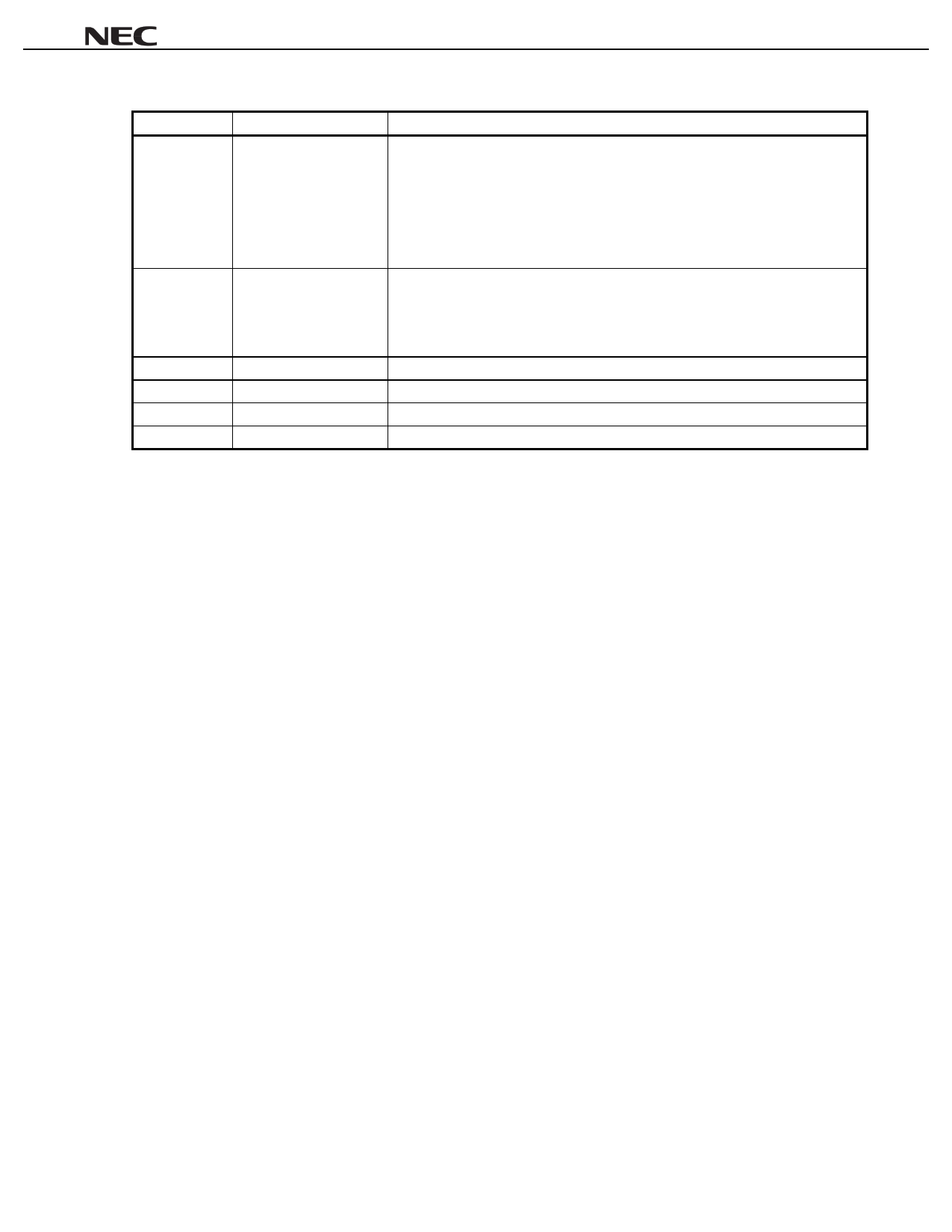
Pin Symbol
Bcont
Pin Name
Bias control
V0 to V9
γ -corrected power
supplies
VDD1
VDD2
VSS1
VSS2
Logic power supply
Driver power supply
Logic ground
Driver ground
Description
(2/2)
This pin can be used to finely control the bias current inside the output amplifier.
In cases when fine-control is necessary, connect this pin to the stabilized ground
potential (VSS2) via an external resistor of 10 to 100kΩ (per IC).
When this fine-control function is not required, leave this pin open.
Refer to 9. CURRENT CONSUMPTION REDUCTION FUNCTION
Input the γ -corrected power supplies from outside by using operational amplifier.
Make sure to maintain the following relationships. During the gray scale voltage
output, be sure to keep the gray scale level power supply at a constant level.
VDD2 – 0.1 V> V0 > V1 > V2 > V3 > V4 > V5 > V6 > V7 > V8 > V9 > VSS2 + 0.1 V
2.3 V to 3.6 V
8.5 V ± 0.5 V
Grounding
Grounding
Cautions 1. The power start sequence must be VDD1, logic input, and VDD2 & V0 to V9 in that order.
Reverse this sequence to shut down. (Simultaneous power application to VDD2 and V0 to V9 is
possible.)
2. To stabilize the supply voltage, please be sure to insert a 0.1 µ F bypass capacitor between
VDD1-VSS1 and VDD2-VSS2. Furthermore, for increased precision of the D/A converter, insertion of a
bypass capacitor of about 0.01 µ F is also advised between the γ -corrected power supply
terminals (V0, V1, V2, ···, V9) and VSS2.
Data Sheet S13972EJ3V0DS00
5
5 Page 
µ PD16732A, 16732B
9. CURRENT CONSUMPTION REDUCTION FUNCTION
The µ PD16732A and 16732B have a low power control function (LPC) which can switch the bias current of the
output amplifier between two levels and a bias control function (Bcont) which can be used to finely control the bias
current.
<Low power control function (LPC)>
The bias current of the output amplifier can be switched between two levels using this pin. (Bcont: Open)
LPC = H or Open: Normal power mode
LPC = L: Low power mode
5 The VDD2 of static current consumption can be reduced to two thirds of that in normal mode. Input a stable DC
current (VDD1/VSS1) to this pin.
<Bias Current Control Function (Bcont)>
It is possible to fine-control the current consumption by using the bias current control function (Bcont pin). When
using this function, connect this pin to the stabilized ground potential (VSS2) via an external resistor (REXT). When
not using this function, leave this pin open.
Refer to the table below for the percentage of current regulation when using the bias current control function.
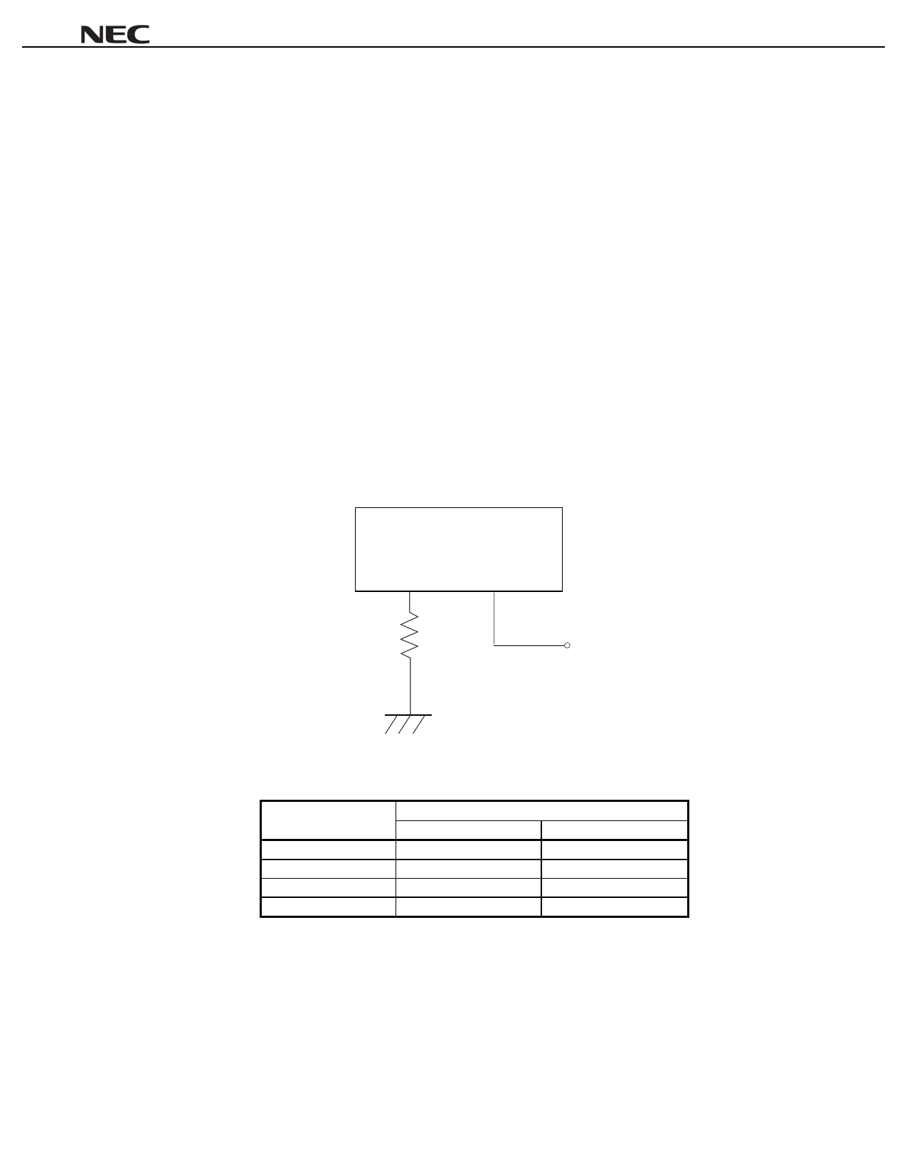
Figure9−1. Bias Current Control Function (Bcont)
µ PD16732A,16732B
Bcont
LPC
REXT
H/L
VSS2
Refer to the table below for the percentage of current regulation when using the bias current control function.
5 Talbe9−1. Current Consumption Regulation Percentage Compared to Normal Mode
REXT
∞ (Open)
50 kΩ
20 kΩ
10 kΩ
Current Consumption Regulation Percentage
LPC = H
LPC = L
100 %
65 %
110 %
70 %
115 %
80 %
120 %
85 %
VDD1 = 3.3 V
VDD2 = 8.7 V
LPC = 3.3 V/0 V
Remark The above current consumption regulation percentages are not product-characteristic guaranteed as they
are based on the results of simulation.
Caution
Because the low-power and bias-current control functions control the bias current in the output
amplifier and regulate the over-all current consumption of the driver IC, when this occurs, the
characteristics of the output amplifier will simultaneously change. Therefore, when using these
functions, be sure to sufficiently evaluate the picture quality.
Data Sheet S13972EJ3V0DS00
11
11 Page | ||
| Páginas | Total 24 Páginas | |
| PDF Descargar | [ Datasheet UPD16732AN.PDF ] | |
Hoja de datos destacado
| Número de pieza | Descripción | Fabricantes |
| UPD16732A | 384-OUTPUT TFT-LCD SOURCE DRIVER COMPATIBLE WITH 64-GRAY SCALES | NEC |
| UPD16732AN | 384-OUTPUT TFT-LCD SOURCE DRIVER COMPATIBLE WITH 64-GRAY SCALES | NEC |
| Número de pieza | Descripción | Fabricantes |
| SLA6805M | High Voltage 3 phase Motor Driver IC. |
Sanken |
| SDC1742 | 12- and 14-Bit Hybrid Synchro / Resolver-to-Digital Converters. |
Analog Devices |
|
DataSheet.es es una pagina web que funciona como un repositorio de manuales o hoja de datos de muchos de los productos más populares, |
| DataSheet.es | 2020 | Privacy Policy | Contacto | Buscar |
