|
|
|
PDF UPA1900 Data sheet ( Hoja de datos )
| Número de pieza | UPA1900 | |
| Descripción | N-CHANNEL MOS FIELD EFFECT TRANSISTOR FOR SWITCHING | |
| Fabricantes | NEC | |
| Logotipo | ||
Hay una vista previa y un enlace de descarga de UPA1900 (archivo pdf) en la parte inferior de esta página. Total 8 Páginas | ||
|
No Preview Available !
DATA SHEET
MOS FIELD EFFECT TRANSISTOR
µ PA1900
N-CHANNEL MOS FIELD EFFECT TRANSISTOR
FOR SWITCHING
DESCRIPTION
The µPA1900 is a switching device which can be driven
directly by a 2.5 V power source.
The µPA1900 features a low on-state resistance and
excellent switching characteristics, and is suitable for
applications such as power switch of portable machine and
so on.
FEATURES
• Can be driven by a 2.5 V power source
• Low on-state resistance
RDS(on)1 = 35 mΩ MAX. (VGS = 4.5 V, ID = 3.0 A)
RDS(on)2 = 38 mΩ MAX. (VGS = 4.0 V, ID = 3.0 A)
RDS(on)3 = 45 mΩ MAX. (VGS = 2.5 V, ID = 3.0 A)
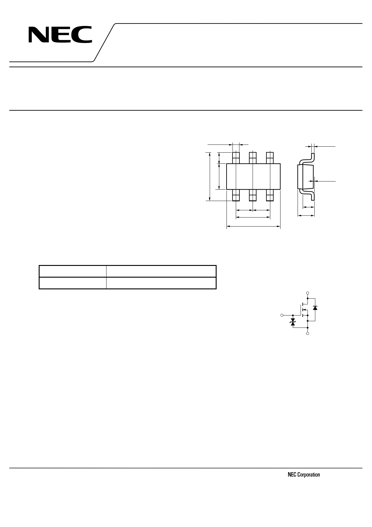
ORDERING INFORMATION
PART NUMBER
µPA1900TE
PACKAGE
6-pin Mini Mold (Thin Type)
PACKAGE DRAWING (Unit : mm)
0.32
+0.1
–0.05
0.16+–00..016
65 4
12 3
0 to 0.1
0.95 0.95
1.9
2.9 ±0.2
0.65
0.9 to 1.1
1, 2, 5, 6 : Drain
3 : Gate
4 : Source
EQUIVALENT CIRCUIT
Drain
ABSOLUTE MAXIMUM RATINGS (TA = 25°C)
Drain to Source Voltage
VDSS
20
Gate to Source Voltage
VGSS
±12
Drain Current (DC)
Drain Current (pulse) Note1
ID(DC)
ID(pulse)
±5.5
±22
Total Power Dissipation
Total Power Dissipation Note2
PT1 0.2
PT2 2
Channel Temperature
Tch 150
Storage Temperature
Tstg –55 to +150
V
V
A
A
W
W
°C
°C
Gate
Body
Diode
Gate
Protection
Diode
Source
Marking: TG
Notes 1. PW ≤ 10 µs, Duty Cycle ≤ 1 %
2. Mounted on FR-4 Board, t ≤ 5 sec.
Remark
The diode connected between the gate and source of the transistor serves as a protector against ESD.
When this device actually used, an additional protection circuit is externally required if a voltage
exceeding the rated voltage may be applied to this device.
The information in this document is subject to change without notice. Before using this document, please
confirm that this is the latest version.
Not all devices/types available in every country. Please check with local NEC representative for
availability and additional information.
Document No. D13809EJ1V0DS00 (1st edition)
Date Published June 1999 NS CP(K)
Printed in Japan
The mark 5 shows major revised points.
© 1998, 1999
1 page 
µ PA1900
1000
100
SWITCHING CHARACTERISTICS
td(off)
tr
tf
td(on)
10
1.0
0.1
VDD = 10 V
VGS(on) = 4.0 V
RG = 10 Ω
1 10
ID - Drain Current - A
SOURCE TO DRAIN DIODE
FORWARD VOLTAGE
100
10
1
0.1
0.01
0.4
0.6 0.8 1.0 1.2 1.4
VF(S-D) - Source to Drain Voltage - V
DYNAMIC INPUT CHARACTERISTICS
10
ID = 5.5 A
8
VDD = 16 V
10 V
6
4
2
0
2 4 6 8 10 12
QG - Gate Charge - nC
TRANSIENT THERMAL RESISTANCE vs. PULSE WIDTH
1000
Single Pulse
Without Board
100
Mounted on 250mm2×35µm Copper Pad
Connected to Drain Electrode
in 50mm×50mm×1.6mm FR-4 Board
10
1
0.001
0.01
0.1 1 10
PW - Pulse Width - s
100 1000
Data Sheet D13809EJ1V0DS00
5
5 Page | ||
| Páginas | Total 8 Páginas | |
| PDF Descargar | [ Datasheet UPA1900.PDF ] | |
Hoja de datos destacado
| Número de pieza | Descripción | Fabricantes |
| UPA1900 | N-CHANNEL MOS FIELD EFFECT TRANSISTOR FOR SWITCHING | NEC |
| Número de pieza | Descripción | Fabricantes |
| SLA6805M | High Voltage 3 phase Motor Driver IC. |
Sanken |
| SDC1742 | 12- and 14-Bit Hybrid Synchro / Resolver-to-Digital Converters. |
Analog Devices |
|
DataSheet.es es una pagina web que funciona como un repositorio de manuales o hoja de datos de muchos de los productos más populares, |
| DataSheet.es | 2020 | Privacy Policy | Contacto | Buscar |