|
|
PDF PCD8544 Data sheet ( Hoja de datos )
| Número de pieza | PCD8544 | |
| Descripción | 48 x 84 pixels matrix LCD controller/driver | |
| Fabricantes | NXP Semiconductors | |
| Logotipo | ||
Hay una vista previa y un enlace de descarga de PCD8544 (archivo pdf) en la parte inferior de esta página. Total 32 Páginas | ||
|
No Preview Available !
INTEGRATED CIRCUITS
DATA SHEET
PCD8544
48 × 84 pixels matrix LCD
controller/driver
Product specification
File under Integrated Circuits, IC17
1999 Apr 12
1 page 
Philips Semiconductors
48 × 84 pixels matrix LCD controller/driver
Product specification
PCD8544
6 PINNING
SYMBOL
DESCRIPTION
R0 to R47
LCD row driver outputs
C0 to C83
LCD column driver outputs
VSS1, VSS2
VDD1, VDD2
VLCD1, VLCD2
T1
ground
supply voltage
LCD supply voltage
test 1 input
T2 test 2 output
T3 test 3 input/output
T4 test 4 input
SDIN
serial data input
SCLK
serial clock input
D/C data/command
SCE
chip enable
OSC
oscillator
RES
external reset input
dummy1, 2, 3, 4 not connected
Note
1. For further details, see Fig.18 and Table 7.
6.1 Pin functions
6.1.1 R0 TO R47 ROW DRIVER OUTPUTS
These pads output the row signals.
6.1.2 C0 TO C83 COLUMN DRIVER OUTPUTS
These pads output the column signals.
6.1.3 VSS1, VSS2: NEGATIVE POWER SUPPLY RAILS
Supply rails VSS1 and VSS2 must be connected together.
6.1.4 VDD1, VDD2: POSITIVE POWER SUPPLY RAILS
Supply rails VDD1 and VDD2 must be connected together.
6.1.5 VLCD1, VLCD2: LCD POWER SUPPLY
Positive power supply for the liquid crystal display. Supply
rails VLCD1 and VLCD2 must be connected together.
6.1.6 T1, T2, T3 AND T4: TEST PADS
T1, T3 and T4 must be connected to VSS, T2 is to be left
open. Not accessible to user.
6.1.7 SDIN: SERIAL DATA LINE
Input for the data line.
6.1.8 SCLK: SERIAL CLOCK LINE
Input for the clock signal: 0.0 to 4.0 Mbits/s.
6.1.9 D/C: MODE SELECT
Input to select either command/address or data input.
6.1.10 SCE: CHIP ENABLE
The enable pin allows data to be clocked in. The signal is
active LOW.
6.1.11 OSC: OSCILLATOR
When the on-chip oscillator is used, this input must be
connected to VDD. An external clock signal, if used, is
connected to this input. If the oscillator and external clock
are both inhibited by connecting the OSC pin to VSS, the
display is not clocked and may be left in a DC state.
To avoid this, the chip should always be put into
Power-down mode before stopping the clock.
6.1.12 RES: RESET
This signal will reset the device and must be applied to
properly initialize the chip. The signal is active LOW.
1999 Apr 12
5
5 Page 
Philips Semiconductors
48 × 84 pixels matrix LCD controller/driver
Product specification
PCD8544
8 INSTRUCTIONS
The instruction format is divided into two modes: If D/C
(mode select) is set LOW, the current byte is interpreted as
command byte (see Table 1). Figure 8 shows an example
of a serial data stream for initializing the chip. If D/C is set
HIGH, the following bytes are stored in the display data
RAM. After every data byte, the address counter is
incremented automatically.
The level of the D/C signal is read during the last bit of data
byte.
Each instruction can be sent in any order to the PCD8544.
The MSB of a byte is transmitted first. Figure 9 shows one
possible command stream, used to set up the LCD driver.
The serial interface is initialized when SCE is HIGH. In this
state, SCLK clock pulses have no effect and no power is
consumed by the serial interface. A negative edge on SCE
enables the serial interface and indicates the start of a data
transmission.
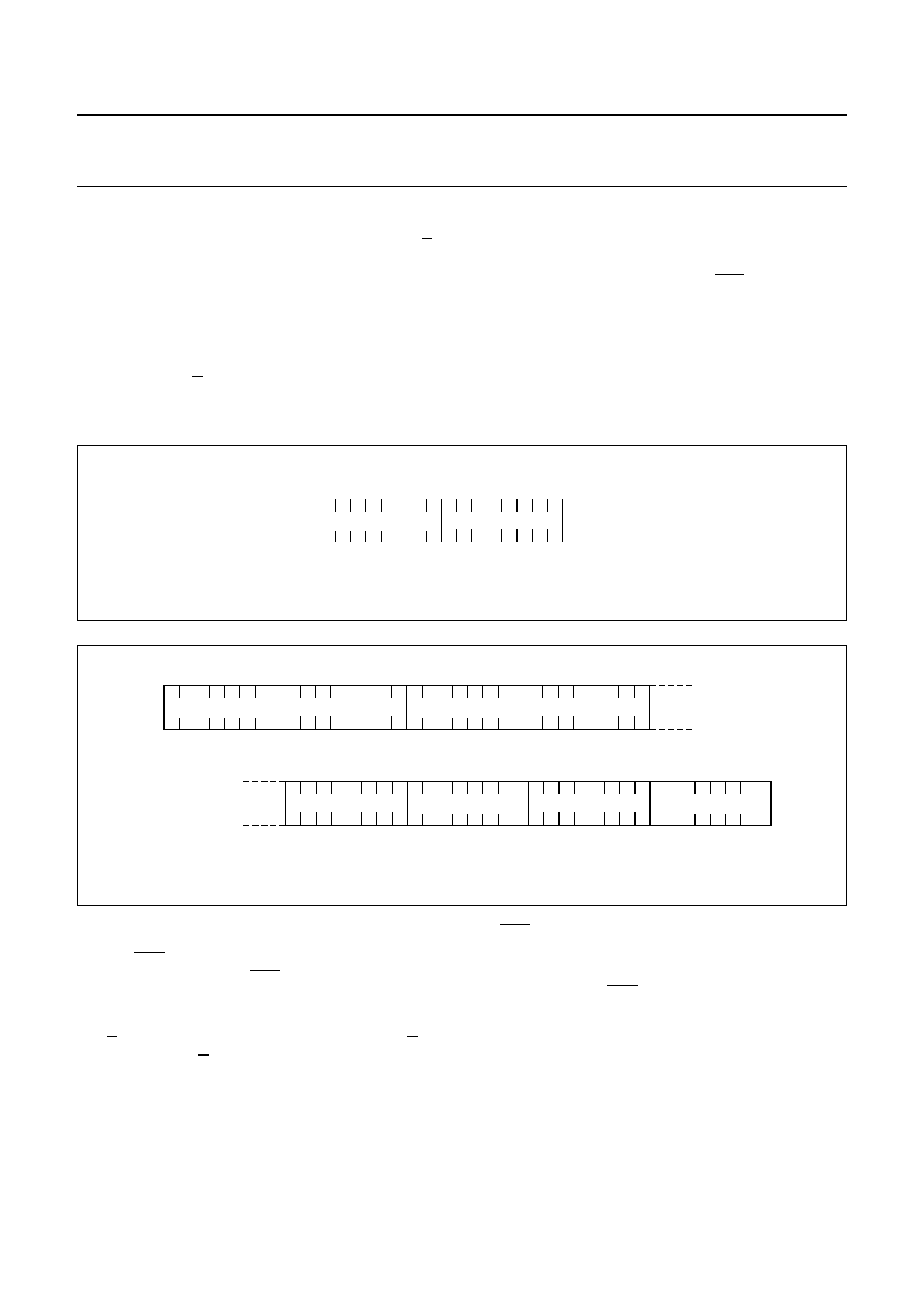
handbookM, hSalBfpa(gDeB7)
data
LSB (DB0)
data
MGL666
Fig.8 General format of data stream.
handbook, full pagewidth
function set (H = 1)
bias system
set VOP
temperature control
function set (H = 0)
display control
Y address
Fig.9 Serial data stream, example.
X address
MGL642
Figures 10 and 11 show the serial bus protocol.
• When SCE is HIGH, SCLK clock signals are ignored;
during the HIGH time of SCE, the serial interface is
initialized (see Fig.12)
• SDIN is sampled at the positive edge of SCLK
• D/C indicates whether the byte is a command (D/C = 0)
or RAM data (D/C = 1); it is read with the eighth SCLK
pulse
• If SCE stays LOW after the last bit of a command/data
byte, the serial interface expects bit 7 of the next byte at
the next positive edge of SCLK (see Fig.12)
• A reset pulse with RES interrupts the transmission.
No data is written into the RAM. The registers are
cleared. If SCE is LOW after the positive edge of RES,
the serial interface is ready to receive bit 7 of a
command/data byte (see Fig.13).
1999 Apr 12
11
11 Page | ||
| Páginas | Total 32 Páginas | |
| PDF Descargar | [ Datasheet PCD8544.PDF ] | |
Hoja de datos destacado
| Número de pieza | Descripción | Fabricantes |
| PCD8544 | 48 x 84 pixels matrix LCD controller/driver | NXP Semiconductors |
| Número de pieza | Descripción | Fabricantes |
| SLA6805M | High Voltage 3 phase Motor Driver IC. |
Sanken |
| SDC1742 | 12- and 14-Bit Hybrid Synchro / Resolver-to-Digital Converters. |
Analog Devices |
|
DataSheet.es es una pagina web que funciona como un repositorio de manuales o hoja de datos de muchos de los productos más populares, |
| DataSheet.es | 2020 | Privacy Policy | Contacto | Buscar |
