|
|
|
PDF PC87415 Data sheet ( Hoja de datos )
| Número de pieza | PC87415 | |
| Descripción | PCI-IDE DMA Master Mode Interface Controller | |
| Fabricantes | National Semiconductor | |
| Logotipo | ||
Hay una vista previa y un enlace de descarga de PC87415 (archivo pdf) en la parte inferior de esta página. Total 30 Páginas | ||
|
No Preview Available !
PRELIMINARY
March 1996
PC87415
PCI-IDE DMA Master Mode Interface Controller
1 0 General Description
The Enhanced PCI-IDE Interface is a single-chip controller
packaged in a 100-pin PQFP It provides 2 IDE channels for
interfacing up to 4 IDE drives or 2 IDE drives and CD-ROM
directly on the PCI Local bus An enhanced DMA controller
on-chip increases system performance by providing full
scatter gather data transfers between IDE devices and sys-
tem memory without CPU intervention Four levels of both
write posting and read prefetching per channel allow the
host CPU to run concurrently with IDE cycles Programma-
ble timing functions provide maximum flexibility of timing pa-
rameters per drive for optimizing the data transfer rate per
drive Both PC compatible addressing and PCI compliant
addressing are supported by re-mapping the base address-
es A power control feature allows turning off power to the
IDE cables
The Enhanced PCI-IDE Interface connection to the PCI bus
is virtually ‘‘glue-less’’ with only one additional TTL data
buffer (optional) This high-integration solution reduces
component count eases board design reduces cost and
increases reliability
The Enhanced PCI-IDE supports faster ATA devices using
PIO modes 1 2 3 and 4 as well as DMA modes 0 1 and 2
It comes with a full suite of software drivers for DOS 5 0 –
6 x Windows 3 x Windows 95 Windows NTTM OS 2
2 x Novell NetWareTM 3 1x – 4 x and SCO UNIX 3 x
TRI-STATE is a registered trademark of National Semiconductor Corporation
WATCHDOGTM is a trademark of National Semiconductor Corporation
Novell is a registered trademark of Novell Inc
NetWareTM is a trademark of Novell Inc
Unix is a registered trademark of AT T Bell Laboratories
Windows and Windows 95 are registered trademarks of Microsoft Corporation
Windows NTTM is a trademark of Microsoft Corporation
2 0 Features
Y PCI bus interface for up to 4 IDE devices
Y 33 MHz 32-bit PCI bus data path with full parity error
reporting
Y 16 7 MByte sec maximum IDE transfer rate
Y Support for 2 IDE channels ( 2 IDE devices per chan-
nel)
Y Primary or secondary IDE addressing (1F0x 170x) in
PC compatible mode
Y Re-mappable base registers for full PCI compliance
Y Concurrent channel operation (PIO DMA modes)
Y 4 Double Word write FIFO per channel
Y 4 Double Word read prefetch FIFO per channel
Y Enhanced DMA mode with scatter gather capability
Y ANSI ATA Modes 0 through 4 PIO support (internal
DMA not selected)
Y IORDY handshaking for PIO
Y ANSI ATA Modes 0 through 2 Multiword DMA support
(internal DMA selected)
Y Individually programmable command and recovery tim-
ing for reads and writes per channel drive for com-
mand control and data
Y Individually programmable data sector size for read pre-
fetches per channel
Y PC compatible interrupt routing of IRQ14 and IRQ15
Y Hardware and software chip enable disable
Y Optional Power Control for IDE Drives
Y Fully static logic design
Y 100-pin PQFP package
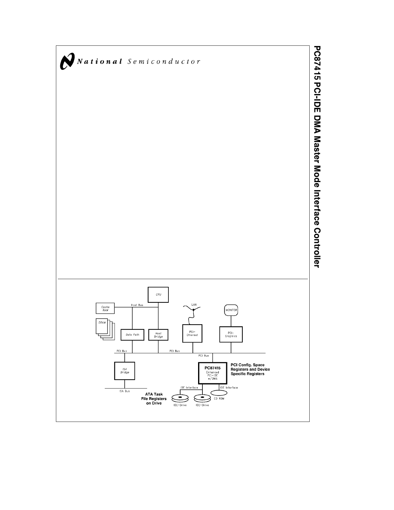
FIGURE 1 The PC87415 in a PCI Based System
C1996 National Semiconductor Corporation TL F 12497
RRD-B30M46 Printed in U S A
TL F 12497 – 1
http www national com
1 page 
4 0 Pin Description (Continued)
4 2 IDE INTERFACE
Name
DD 15 0
DA 0
TEST
DA 1
ENABLE
DA 2
LEGACY
DIORDY
DIOR
DIOW
DRST
CH1 CS1
CH1 CS3
CH2 CS1
CH2 CS3
CH1 INTRQ
CH2 INTRQ
CH1
DMARQ
CH2
DMARQ
CH1
DMACK
CH2
DMACK
IRQ14
IRQ15
Type
IO
IO
IO
IO
I
O
O
O
O
O
I
I
I
O
O
O
O
Description
DRIVE DATA BUS The 16-bit bi-directional data bus to the drive The lower 8 bits are used for non data
8-bit transfers (e g registers ECC bytes)
DRIVE ADDRESS LINE 0 OR TEST The DA0 address line is asserted by the host to access a register or
data port in the drive It may also be used for testing during PCI Reset the rising edge of RST samples
this pin If ‘‘low’’ all device output pins are forced to a TRI-STATE level
DRIVE ADDRESS LINE 1 OR ENABLE During normal operation the DA1 address line is asserted by the
host to access a register or data port in the drive During PCI Reset the rising edge of RST samples this
pin and places its value in the Command Register bit-0
DRIVE ADDRESS LINE 2 OR LEGACY Dining normal operation the DA2 address line is asserted by the
host to access a register or data port in the drive During PCI Reset the rising edge of RST samples this
pin and places its value in the Programming Interface Register bits 0 and 2
DRIVE I O CHANNEL READY When the drive is not ready to respond to a data transfer request this
signal is negated (low) to extend the disk transfer cycle of any register access (read or write) When
DIORDY is not negated it remains in a high impedance state
DRIVE I O READ The read strobe signal for both channels The falling edge of DIOR enables data from
a register or the data port of the drive onto the PCI-IDE chip
DRIVE I O WRITE The write strobe signal for both channels The rising edge of DIOW clocks data from
the PCI-IDE chip into the register or the data port of the drive
DRIVE RESET This signal from the PCI-IDE chip is asserted after power up or under software control (see
Control Register bits Table A) It is active for as long as the PCI Reset signal or if the reset bit in the
Control Register is set
CHANNEL 1 CHIP SELECT 1 AND 3 CH1 CS1 is the chip select signal to select the Command Block
Registers CH1 CS3 is the chip select signal to select the Control Block Registers
CHANNEL 2 CHIP SELECT 1 AND 3 CH2 CS1 is the chip select signal to select the Command Block
Registers CH2 CS3 is the chip select signal to select the Control Block Registers
DRIVE INTERRUPTS These signals are used to interrupt the host system CH1 INTRQ is asserted only
when the drive(s) on channel 1 has a pending interrupt and the host has cleared nIEN in the drive’s
Device Control Register CH2 INTRQ is asserted only when the drive(s) on channel 2 has a pending
interrupt and the host has cleared nIEN in the Device Control Register
CHANNEL 1 DMA REQUEST This signal is used when using the internal DMA controller When this
signal is asserted the selected drive on channel 1 is ready to transfer data
CHANNEL 2 DMA REQUEST This signal is used when using the internal DMA controller When this
signal is asserted the selected drive on channel 2 is ready to transfer data
CHANNEL 1 DMA ACKNOWLEDGE This signal is used when using the internal DMA controller When
asserted it signals the selected drive on channel 1 that data has been accepted or that data is available
CHANNEL 2 DMA ACKNOWLEDGE This signal is used when using the internal DMA controller When
asserted it signals the selected drive on channel 2 that data has been accepted or that data is available
IRQ14 mirrors CH1 INT if Legacy mode is enabled
IRQ15 mirrors CH2 INT if Legacy mode is enabled
5 http www national com
5 Page 
5 0 Configuration Registers (Continued)
Reg
(HEX)
40 – 42
RW
Description
RW
CONTROL REGISTER (CTRL) Default value is 00000000h (after Reset)
Bit 0
Bit 1
Bit 2
Bit 3
Reserved
0 (Always) Reserved
0 e Software reset to CH1 CH2 off
1 e Software reset to CH1 CH2 on
0 e IDE PWR set on
1 e IDE PWR set off
Note Bit 18 must be set to ‘‘1’’ to allow Bit 3 to toggle IDE PWR
B18 B3
0X
10
11
IDE PWR
1 (Default at power up reset)
1 (IDE PWR set to on)
0 (IDE PWR set to off)
( ) Asserted for t 25 s
Bit 4 0 e Map CH1 INT according to legacy native mapping scheme
1 e Map CH1 INT to INTA regardless if in legacy mode
Bit 5 0 e Map CH2 INT according to legacy native mapping scheme
1 e Map CH2 INT to INTA regardless if in legacy mode
Bit 6 0 e INTA unmasked
1 e INTA masked
Bit 7 0 e Write to vendor ID and device ID registers disabled
1 e Write to vendor ID and device ID registers enabled
Bit 8 0 e Channel 1 interrupt unmasked
1 e Channel 1 interrupt masked
Bit 9 0 e Channel 2 interrupt unmasked
1 e Channel 2 interrupt masked
Bit 10 0 e PCI Base Address Register 2 and 3 enabled
1 e PCI Base Address Register 2 and 3 disabled
Bit 11 0 e PCI data phase WATCHDOGTM timer disabled
1 e PCI data phase WATCHDOG timer enabled
11 http www national com
11 Page | ||
| Páginas | Total 30 Páginas | |
| PDF Descargar | [ Datasheet PC87415.PDF ] | |
Hoja de datos destacado
| Número de pieza | Descripción | Fabricantes |
| PC87410 | PC87410 PCI-IDE Interface Controller | National Semiconductor |
| PC87410VLK | PC87410 PCI-IDE Interface Controller | National Semiconductor |
| PC87413 | LPC ServerI/O for Servers and Workstations | National Semiconductor |
| PC87414 | LPC ServerI/O for Servers and Workstations | National Semiconductor |
| Número de pieza | Descripción | Fabricantes |
| SLA6805M | High Voltage 3 phase Motor Driver IC. |
Sanken |
| SDC1742 | 12- and 14-Bit Hybrid Synchro / Resolver-to-Digital Converters. |
Analog Devices |
|
DataSheet.es es una pagina web que funciona como un repositorio de manuales o hoja de datos de muchos de los productos más populares, |
| DataSheet.es | 2020 | Privacy Policy | Contacto | Buscar |