|
|
|
PDF IDT74LVC125ADC Data sheet ( Hoja de datos )
| Número de pieza | IDT74LVC125ADC | |
| Descripción | 3.3V CMOS QUADRUPLE BUS BUFFER GATE WITH 3-STATE OUTPUTS AND 5 VOLT TOLERANT I/O | |
| Fabricantes | Integrated Device | |
| Logotipo | ||
Hay una vista previa y un enlace de descarga de IDT74LVC125ADC (archivo pdf) en la parte inferior de esta página. Total 6 Páginas | ||
|
No Preview Available !
IDT74LVC125A
3.3VCMOSQUADRUPLE BUS BUFFER GATE WITH 3-STATE OUTPUTS
3.3V CMOS QUADRUPLE
BUS BUFFER GATE
WITH 3-STATE OUTPUTS
AND 5 VOLT TOLERANT I/O
INDUSTRIALTEMPERATURERANGE
IDT74LVC125A
FEATURES:
• 0.5 MICRON CMOS Technology
• ESD > 2000V per MIL-STD-883, Method 3015; > 200V using
machine model (C = 200pF, R = 0)
• VCC = 3.3V ± 0.3V, Normal Range
• VCC = 2.7V to 3.6V, Extended Range
• CMOS power levels (0.4µ W typ. static)
• Rail-to-Rail output swing for increased noise margin
• All inputs, outputs, and I/Os are 5V tolerant
• Supports hot insertion
• Available in SOIC, SSOP, and TSSOP packages
DRIVE FEATURES:
• High Output Drivers: ±24mA
• Reduced system switching noise
DESCRIPTION:
The LVC125A quadruple bus buffer gate is built using advanced dual
metal CMOS technology. The LVC125A features independent line drivers
with 3-state outputs. Each output is disabled when the associated output-
enable (OE) input is high.
To ensure the high impedance state during power up or power down,
OE should be tied to Vcc through a pullup resistor; the minimum value of the
resistor is determined by the current-sinking capability of the driver.
Inputs can be driven from either 3.3V or 5V devices. This feature allows
the use of this device as a translator in a mixed 3.3V/5V system environment.
The LVC125A has been designed with a ±24mA output driver. This
driver is capable of driving a moderate to heavy load while maintaining
speed performance.
APPLICATIONS:
• 5V and 3.3V mixed voltage systems
• Data communication and telecommunication systems
FUNCTIONAL BLOCK DIAGRAM
1OE
1
2
1A
2OE 4
5
2A
3
1Y
6 2Y
3OE
10
9
3A
4OE 13
12
4A
8
3Y
11 4Y
The IDT logo is a registered trademark of Integrated Device Technology, Inc.
INDUSTRIAL TEMPERATURE RANGE
©2000 Integrated Device Technology, Inc.
1
FEBRUARY 2000
DSC-4557/1
1 page 
IDT74LVC125A
3.3VCMOSQUADRUPLE BUS BUFFER GATE WITH 3-STATE OUTPUTS
INDUSTRIALTEMPERATURERANGE
TEST CIRCUITS AND WAVEFORMS
TEST CONDITIONS
Symbol
VCC(1)= 2.5V±0.2V
VLOAD
2 x Vcc
VIH Vcc
VT Vcc / 2
VLZ 150
VHZ 150
CL 30
VCC(2)= 3.3V±0.3V & 2.7V
6
2.7
1.5
300
300
50
Unit
V
V
V
mV
mV
pF
SAME PHASE
INPUT TRANSITION
OUTPUT
tPLH
OPPOSITE PHASE
INPUT TRANSITION
tPLH
tPHL
tPHL
Propagation Delay
VIH
VT
0V
VOH
VT
VOL
VIH
VT
0V
LVC QUAD Link
Pulse(1, 2)
Generator
VIN
VCC
VOUT
D.U.T.
500Ω
VLOAD
Open
GND
RT
500Ω
CL
Test Circuit for All Outputs
LVC QUAD Link
DEFINITIONS:
CL = Load capacitance: includes jig and probe capacitance.
RT = Termination resistance: should be equal to ZOUT of the Pulse Generator.
NOTES:
1. Pulse Generator for All Pulses: Rate ≤ 10MHz; tF ≤ 2ns; tR ≤ 2ns.
2. Pulse Generator for All Pulses: Rate ≤ 10MHz; tF ≤ 2.5ns; tR ≤ 2.5ns.
SWITCH POSITION
Test
Open Drain
Disable Low
Enable Low
Disable High
Enable High
All Other Tests
Switch
VLOAD
GND
Open
INPUT
OUTPUT 1
OUTPUT 2
tPLH1
tPHL1
tSK (x)
tSK (x)
VIH
VT
0V
VOH
VT
VOL
VOH
VT
VOL
tPLH2
tPHL2
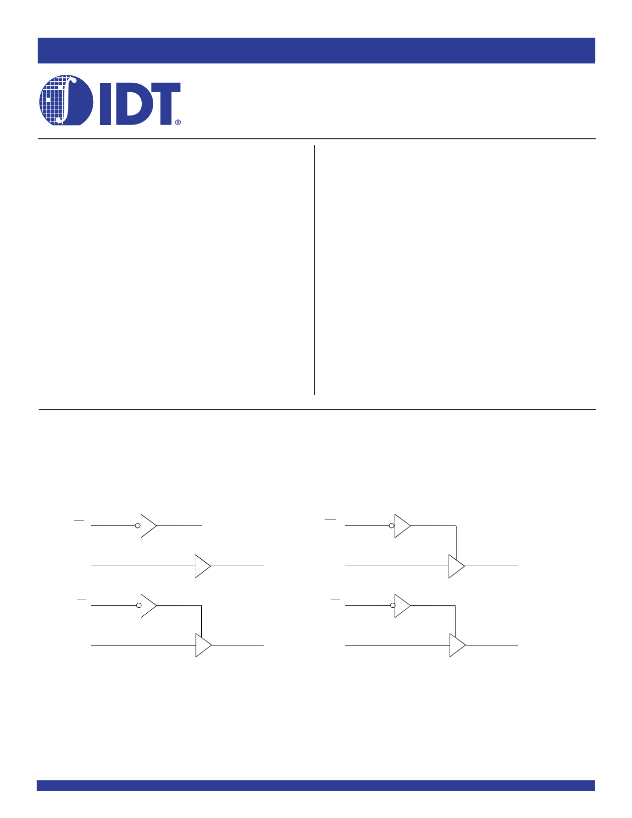
tSK(x) = tPLH2 - tPLH1 or tPHL2 - tPHL1
Output Skew - tSK(X)
LVC QUAD Link
NOTES:
1. For tSK(o) OUTPUT1 and OUTPUT2 are any two outputs.
2. For tSK(b) OUTPUT1 and OUTPUT2 are in the same bank.
CONTROL
INPUT
ENABLE
tPZL
DISABLE
tPLZ
OUTPUT
NORMALLY
SWITCH
CLOSED
LOW
tPZH
OUTPUT
NORMALLY
HIGH
SWITCH
OPEN
VLOAD/2
VT
tPHZ
VT
0V
VIH
VT
0V
VLOAD/2
VLZ
VOL
VOH
VHZ
0V
LVC QUAD Link
NOTE:
1. Diagram shown for input Control Enable-LOW and input Control Disable-HIGH.
Enable and Disable Times
DATA
INPUT
TIMING
INPUT
SYNCHRONOUS
CONTROL
ASYNCHRONOUS
CONTROL
tSU tH
tREM
tSU tH
VIH
VT
0V
VIH
VT
0V
VIH
VT
0V
VIH
VT
0V
LVC QUAD Link
Set-up, Hold, and Release Times
LOW-HIGH-LOW
PULSE
HIGH-LOW-HIGH
PULSE
tW
Pulse Width
VT
VT
LVC QUAD Link
5
5 Page | ||
| Páginas | Total 6 Páginas | |
| PDF Descargar | [ Datasheet IDT74LVC125ADC.PDF ] | |
Hoja de datos destacado
| Número de pieza | Descripción | Fabricantes |
| IDT74LVC125ADC | 3.3V CMOS QUADRUPLE BUS BUFFER GATE WITH 3-STATE OUTPUTS AND 5 VOLT TOLERANT I/O | Integrated Device |
| Número de pieza | Descripción | Fabricantes |
| SLA6805M | High Voltage 3 phase Motor Driver IC. |
Sanken |
| SDC1742 | 12- and 14-Bit Hybrid Synchro / Resolver-to-Digital Converters. |
Analog Devices |
|
DataSheet.es es una pagina web que funciona como un repositorio de manuales o hoja de datos de muchos de los productos más populares, |
| DataSheet.es | 2020 | Privacy Policy | Contacto | Buscar |