|
|
|
PDF PC87363 Data sheet ( Hoja de datos )
| Número de pieza | PC87363 | |
| Descripción | 128-Pin LPC SuperI/O with MIDI and Game Ports/ Extended Wake-Up and Protection | |
| Fabricantes | National Semiconductor | |
| Logotipo | ||
Hay una vista previa y un enlace de descarga de PC87363 (archivo pdf) en la parte inferior de esta página. Total 30 Páginas | ||
|
No Preview Available !
PRELIMINARY
January 10, 1999
PC87363
128-Pin LPC SuperI/O with MIDI and Game Ports, Extended
Wake-Up and Protection
General Description
The PC87363, a member of National Semiconductor’s 128-
pin LPC SuperI/O family, introduces a Musical Instrument
Digital Interface (MIDI) Port and Game Port inputs for up to
two game devices. It also offers wake-up support for a wide
range of wake-up events, and new hardware and software
features to protect the system design. Like all members of
this family, it is PC99 and ACPI compliant, and offers a single-
chip solution to the most commonly used PC I/O peripherals.
The PC87363 also incorporates: Fan Speed Control and
Monitoring for two fans, a Floppy Disk Controller (FDC), a
Keyboard and Mouse Controller (KBC), a full IEEE 1284
Parallel Port, two enhanced Serial Ports (UARTs), one with
Infrared (IR) support, ACCESS.bus® Interface (ACB), Sys-
tem Wake-Up Control (SWC), General-Purpose Input/Out-
put (GPIO) support for a total of 49 ports and an enhanced
WATCHDOG™ timer.
Outstanding Features
q MIDI Port compatible with MPU-401 UART mode
q Game Port inputs for up to two game devices
q Extended Wake-Up support, including legacy/ACPI
power button support, direct power supply control in
response to wake-up events, power-fail recovery
q Protection features, including chassis intrusion detection,
GPIO lock and pin configuration lock
q Serial IRQ support (15 options)
q Bus interface, based on Intel’s LPC Interface Specifi-
cation Revision 1.0, September 29th, 1997
q Fan Speed Control and Monitor for two fans
q ACCESS.bus Interface, SMBus physical layer compatible
q 49 GPIO Ports (37 standard, including 23 with Assert
IRQ/SMI/PWUREQs interrupts; 12 VSB-powered)
q Blinking LEDs
q 128-pin PQFP Package
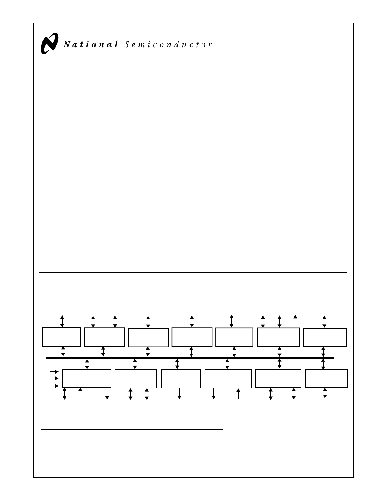
Block Diagram
Serial
Serial Infrared
Interface Interface Interface
I/O
Ports
Floppy Drive Parallel Port LPC Serial
Game Device
Interface
Interface Interface IRQ SMI
Interface
Serial Port 1
Serial Port 2
with IR
GPIO Ports
Floppy Disk IEEE 1284
Controller Parallel Port
Bus
Interface
Game Port
VDD
VBAT
VSB
System Wake-Up ACCESS.bus WATCHDOG
Fan Speed
Keyboard &
Control
Interface
Timer
Control & Monitor Mouse Controller
Power Wake-Up PWUREQ SCL SDA
Control Events
WDO
2 Control 2 Monitor Keyboard & Ports
Outputs Inputs Mouse I/F
MIDI Port
MIDI
Interface
ACCESS.bus® is a registered trademark of Digital Equipment Corporation.
I2C® is a registered trademark of Philips Corporation.
IBM®, MicroChannel®, PC-AT® and PS/2® are registered trademarks of International Business Machines Corporation.
Microsoft® and Windows® are registered trademarks of Microsoft Corporation.
TRI-STATE® is a registered trademark of National Semiconductor Corporation.
WATCHDOG‰ is a trademark of National Semiconductor Corporation.
SMBus® is a registered trademark of Intel Corporation.
© 1999 National Semiconductor Corporation
www.national.com
1 page 
Table of Contents
Datasheet Revision Record .................................................................................................................... 4
1.0 Signal/Pin Connection and Description
1.1 CONNECTION DIAGRAM ......................................................................................................... 13
1.2 BUFFER TYPES AND SIGNAL/PIN DIRECTORY .................................................................... 14
1.3 PIN MULTIPLEXING ................................................................................................................. 19
1.4 DETAILED SIGNAL/PIN DESCRIPTIONS ................................................................................ 21
1.4.1 ACCESS.bus Interface (ACB) .................................................................................... 21
1.4.2 Bus Interface ............................................................................................................... 21
1.4.3 Clock ............................................................................................................................ 21
1.4.4 Fan Speed Control and Monitor (FSCM) ..................................................................... 21
1.4.5 Floppy Disk Controller (FDC) ...................................................................................... 22
1.4.6 Game Port .................................................................................................................. 23
1.4.7 General-Purpose Input/Output (GPIO) Ports ............................................................... 23
1.4.8 Infrared (IR) ................................................................................................................. 23
1.4.9 Keyboard and Mouse Controller (KBC) ..................................................................... 24
1.4.10 Musical Instrument Digital Interface (MIDI) Port .......................................................... 24
1.4.11 Parallel Port ............................................................................................................... 25
1.4.12 Power and Ground ..................................................................................................... 26
1.4.13 Protection .................................................................................................................... 26
1.4.14 Serial Port 1 and Serial Port 2 ..................................................................................... 26
1.4.15 Strap Configuration ...................................................................................................... 27
1.4.16 System Wake-Up Control ............................................................................................ 27
1.4.17 WATCHDOG Timer (WDT) ......................................................................................... 28
1.5 INTERNAL PULL-UP AND PULL-DOWN RESISTORS ............................................................ 29
2.0 Device Architecture and Configuration
2.1 OVERVIEW ............................................................................................................................... 31
2.2 CONFIGURATION STRUCTURE AND ACCESS ..................................................................... 31
2.2.1 The Index-Data Register Pair ...................................................................................... 31
2.2.2 Banked Logical Device Registers Structure ................................................................ 33
2.2.3 Standard Logical Device Configuration Register Definitions ....................................... 34
2.2.4 Standard Configuration Registers ............................................................................... 36
2.2.5 Default Configuration Setup ........................................................................................ 37
2.2.6 Power States ............................................................................................................... 37
2.2.7 Address Decoding ....................................................................................................... 38
2.3 PROTECTION ........................................................................................................................... 38
2.3.1 Chassis Intrusion Detection ......................................................................................... 38
2.3.2 Pin Configuration Lock ................................................................................................ 38
2.3.3 GPIO Pin Function Lock .............................................................................................. 39
2.4 POWER SUPPLY CONTROL (PSC) ......................................................................................... 39
2.5 LED OPERATION AND STATES .............................................................................................. 41
2.6 POWER SUPPLY CONTROL AND LED CONFIGURATION .................................................... 41
2.7 REGISTER TYPE ABBREVIATIONS ........................................................................................ 42
5 www.national.com
5 Page 
Table of Contents (Continued)
11.0 Legacy Functional Blocks
11.1 KEYBOARD AND MOUSE CONTROLLER (KBC) .................................................................. 172
11.1.1 General Description ................................................................................................... 172
11.1.2 KBC Register Map ..................................................................................................... 172
11.1.3 KBC Bitmap Summary ............................................................................................... 172
11.2 FLOPPY DISK CONTROLLER (FDC) ..................................................................................... 173
11.2.1 General Description ................................................................................................... 173
11.2.2 FDC Register Map ..................................................................................................... 173
11.2.3 FDC Bitmap Summary ............................................................................................... 174
11.3 PARALLEL PORT .................................................................................................................... 175
11.3.1 General Description ................................................................................................... 175
11.3.2 Parallel Port Register Map ......................................................................................... 175
11.3.3 Parallel Port Bitmap Summary .................................................................................. 176
11.4 UART FUNCTIONALITY (SP1 AND SP2) ............................................................................... 178
11.4.1 General Description ................................................................................................... 178
11.4.2 UART Mode Register Bank Overview ....................................................................... 178
11.4.3 SP1 and SP2 Register Maps for UART Functionality ................................................ 179
11.4.4 SP1 and SP2 Bitmap Summary for UART Functionality ........................................... 181
11.5 IR FUNCTIONALITY (SP2) ..................................................................................................... 183
11.5.1 General Description ................................................................................................... 183
11.5.2 IR Mode Register Bank Overview ............................................................................. 183
11.5.3 SP2 Register Map for IR Functionality ...................................................................... 184
11.5.4 SP2 Bitmap Summary for IR Functionality ................................................................ 185
12.0 Device Characteristics
12.1 GENERAL DC ELECTRICAL CHARACTERISTICS ............................................................... 187
12.1.1 Recommended Operating Conditions ....................................................................... 187
12.1.2 Absolute Maximum Ratings ....................................................................................... 187
12.1.3 Capacitance .............................................................................................................. 187
12.1.4 Power Consumption under Recommended Operating Conditions ............................ 188
12.2 DC CHARACTERISTICS OF PINS, BY I/O BUFFER TYPES ................................................ 188
12.2.1 Input, CMOS Compatible ........................................................................................... 188
12.2.2 Input, PCI 3.3V .......................................................................................................... 188
12.2.3 Input, SMBus Compatible .......................................................................................... 189
12.2.4 Input, Strap Pin .......................................................................................................... 189
12.2.5 Input, TTL Compatible ............................................................................................... 189
12.2.6 Input, TTL Compatible with Schmitt Trigger .............................................................. 189
12.2.7 Output, PCI 3.3V ....................................................................................................... 190
12.2.8 Output, Totem-Pole Buffer ......................................................................................... 190
12.2.9 Output, Open-Drain Buffer ......................................................................................... 190
12.2.10 Exceptions ................................................................................................................. 190
12.3 INTERNAL RESISTORS ......................................................................................................... 191
12.3.1 Pull-Up Resistor ......................................................................................................... 191
12.3.2 Pull-Down Resistor .................................................................................................... 191
11 www.national.com
11 Page | ||
| Páginas | Total 30 Páginas | |
| PDF Descargar | [ Datasheet PC87363.PDF ] | |
Hoja de datos destacado
| Número de pieza | Descripción | Fabricantes |
| PC87360 | 128-Pin LPC SuperI/O with Protection and Extensive GPIO Support | National Semiconductor |
| PC87363 | 128-Pin LPC SuperI/O with MIDI and Game Ports/ Extended Wake-Up and Protection | National Semiconductor |
| PC87364 | 128-Pin LPC SuperI/O with Extended Wake-Up and Protection Support | National Semiconductor |
| PC87365 | 128-Pin LPC SuperI/O with System Hardware Monitoring | National Semiconductor |
| Número de pieza | Descripción | Fabricantes |
| SLA6805M | High Voltage 3 phase Motor Driver IC. |
Sanken |
| SDC1742 | 12- and 14-Bit Hybrid Synchro / Resolver-to-Digital Converters. |
Analog Devices |
|
DataSheet.es es una pagina web que funciona como un repositorio de manuales o hoja de datos de muchos de los productos más populares, |
| DataSheet.es | 2020 | Privacy Policy | Contacto | Buscar |