|
|
|
PDF PC87306VUL Data sheet ( Hoja de datos )
| Número de pieza | PC87306VUL | |
| Descripción | PC87306 SuperI/OTM Enhanced Sidewinder Lite Floppy Disk Controller/ Keyboard Controller/ Real-Time Clock/ Dual UARTs/ Infrared Interface/ IEEE 1284 Pa | |
| Fabricantes | National Semiconductor | |
| Logotipo | ||
Hay una vista previa y un enlace de descarga de PC87306VUL (archivo pdf) en la parte inferior de esta página. Total 30 Páginas | ||
|
No Preview Available !
PRELIMINARY
November 1995
PC87306 SuperI OTM Enhanced Sidewinder Lite
Floppy Disk Controller Keyboard Controller
Real-Time Clock Dual UARTs Infrared Interface
IEEE 1284 Parallel Port and IDE Interface
General Description
The PC87306 is a single chip solution incorporating a Key-
board and PS 2 Mouse Controller (KBC) Real Time Clock
(RTC) and most commonly used I O peripherals in ISA
EISA and MicroChannel based computers In addition to
the KBC and RTC a Floppy Disk Controller (FDC) two full
featured UARTs an IEEE 1284 compatible parallel port and
all the necessary control logic for an IDE interface provides
support for most commonly used I O peripherals Standard
PC-AT address decoding for all the peripherals a set of
configuration registers and two user selectable chip selects
are also implemented in this highly integrated member of
the SuperI O family The advanced features and high inte-
gration of the PC87306 result in several benefits for low
cost high performance systems Printed circuit board space
savings fewer components on the motherboard and com-
patibility with the latest industry standard peripherals are
only a few of the benefits of using a PC87306
The KBC is fully software compatible with the 8042AH mi-
crocontroller It contains system timing control logic cus-
tom ROM program memory RAM data memory and 18 pro-
grammable I O lines necessary to implement dedicated
control functions It is an efficient controller which uses pre-
dominantly single byte instructions with support for binary and
BCD arithmetic and extensive bit handling capabilities
(Continued)
Features
Y Floppy Disk Controller
Software compatible with the DP8477 the 765A and
the N82077
16-byte FIFO (disabled by default)
Burst and Non-Burst modes
Perpendicular recording drive support
High performance internal analog data separator
(no external filter components required)
Low power CMOS with power-down mode
Automatic media-sense support with full IBM TDR
(Tape Drive Register) implementation for PC-AT and
PS 2 floppy drive types
Y Keyboard Controller
8042AH and PC87911 software compatible
8-bit Microcomputer with 2 kBytes custom ROM and
256 Bytes data RAM
Asynchronous access to two data registers and one
status register during normal operation
Dedicated open drain outputs for keyboard controller
application
Supports both interrupt and polling
10 programmable I O pins
4 dedicated open-drain bidirectional pins
8-bit Timer Counter
Binary and BCD arithmetic
(Continued)
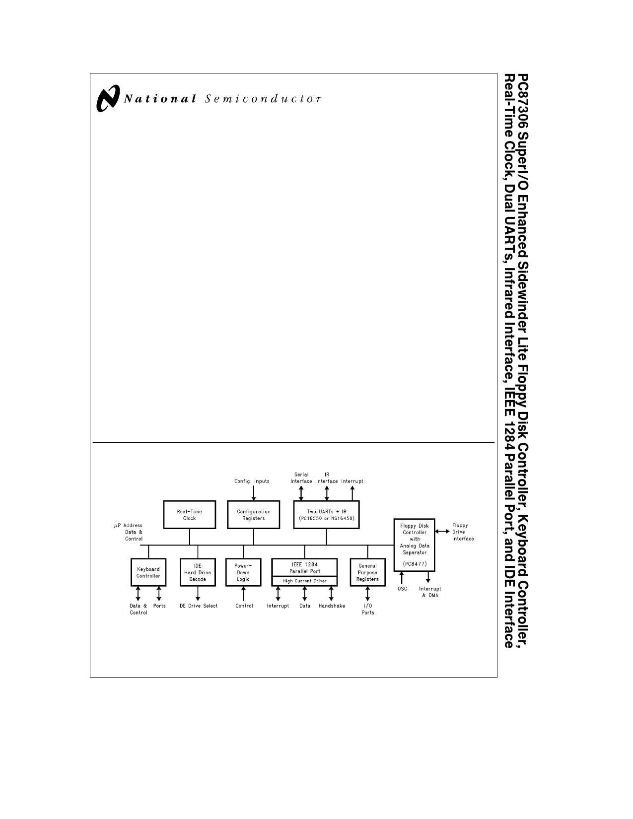
Block Diagram
TRI-STATE is a registered trademark of National Semiconductor Corporation
SuperI OTM is a trademark of National Semiconductor Corporation
MicroChannel PC-AT and PS 2 are registered trademarks of International Business Machines Corporation
C1995 National Semiconductor Corporation TL C 12379
TL C 12379 – 1
RRD-B30M115 Printed in U S A
1 page 
List of Figures
FIGURE 1-1
FIGURE 1-2
FIGURE 2-1
FIGURE 2-2
FIGURE 3-1
FIGURE 4-1
FIGURE 4-2
FIGURE 5-1
FIGURE 5-2
FIGURE 5-3
FIGURE 5-4
FIGURE 6-1
FIGURE 6-2
FIGURE 7-1
FIGURE 8-1
FIGURE 8-2
FIGURE 8-3
FIGURE 8-4
FIGURE 8-5
FIGURE 8-6
FIGURE 8-7
FIGURE 9-1
FIGURE 10-1
FIGURE 10-2
FIGURE 10-3
FIGURE 10-4
FIGURE 10-5
FIGURE 10-7
FIGURE 10-6
FIGURE 10-8
FIGURE 10-9
FIGURE 10-10
FIGURE 10-11
FIGURE 10-12
FIGURE 10-13
FIGURE 10-14
FIGURE 10-15
FIGURE 10-16
FIGURE 11-1
FIGURE 12-1
FIGURE 12-2
FIGURE 12-3
FIGURE 12-4
FIGURE 12-5
FIGURE 12-6
FIGURE 12-7
FIGURE 12-8
FIGURE 12-9
FIGURE 12-10
FIGURE 12-11
FIGURE 12-12
FIGURE 12-13
FIGURE 12-14
Pins Which Utilize the Strap Function during Reset
Multi-Function Pins
PC87306 Configuration Registers
PC87306 Four Floppy Drive Circuit
FDC Functional Block Diagram
FDC Command Structure
IBM Perpendicular and ISO Formats Supported by the Format Command
FDC Data Separator Block Diagram
PC87306 Dynamic Window Margin Performance
Read Data Algorithm State Diagram
Perpendicular Recording Drive R W Head and Pre-Erase Head
PC87306 Composite Serial Data
Receiver FIFO Trigger Level
UART2 Serial and IR Interface Block Diagram
EPP 1 7 Address Write
EPP 1 7 Address Read
EPP Write with ZWS
EPP 1 9 Address Write
EPP 1 9 Address Read
ECP Forward Write Cycle
ECP Backward Read Cycle
IDE Interface Signal Equations (Non-DMA)
Keyboard Controller Functional Block Diagram
Keyboard Controller to Host System Interface
Status Register
Fast IRQ Latching and Clearing
Keyboard Controller Data Memory Map
PSW Register Bits
Keyboard Controller Stack Organization
Active Pull-Up I O Port Structure
Using Port Pins as Inputs
Timing Generation and Timer Circuit
External Clock Connection
Instruction Cycle Timing
Oscillator Internal and External Circuitry
Interrupt Status Timing
Typical Battery Configuration
Typical Battery Current during Battery Backed Mode
General Purpose I O (GPIO) Ports
Clock Timing
Microprocessor Read Timing
Microprocessor Write Timing
Read after Write Operation to All Registers and RAM Timing
Baud Out Timing
Transmitter Timing
Receiver Timing
FIFO Mode Receiver Timing
Timeout Receiver Timing
MODEM Control Timing
FDC DMA Timing
ECP DMA Timing
Reset Timing
Write Data Timing
5
5 Page 
1 0 Pin Description (Continued)
TABLE 1-1 Pin Descriptions (Alphabetical) (Continued)
Symbol
Pin I O
Function
DIR 69 O FDC Direction This output determines the direction of the floppy disk drive (FDD) head
movement (active e step in inactive e step out) during a seek operation During reads or writes
DIR is inactive
DR0 1
73 74
O FDC Drive Select 0 1 These are the decoded Drive Select outputs that are controlled by the
Digital Output Register bits D0 D1 The Drive Select outputs are gated with DOR bits 4 – 7 These
are active low outputs They are encoded with information to control four FDDs when bit 4 of the
Function Enable Register (FER) is set (See MTR0 1 for more information )
DRATE0 1 82 81
O FDC Data Rate 0 1 These outputs reflect the currently selected FDC data rate (bits 0 and 1 in
the Configuration Control Register (CCR) or the Data Rate Select Register (DSR) whichever was
written to last) These pins are totem-pole buffered outputs (6 mA sink 6 mA source)
DSKCHG
71 I FDC Disk Change This input indicates if the drive door has been opened The state of this pin is
available from the Digital Input register This pin can also be configured as the Read Gate
(RGATE) data separator diagnostic input via the Mode command (see Section 4 2 6)
DSR1 2
111 103
I UARTs Data Set Ready When low this signal indicates that the data set or MODEM is ready to
establish a communications link The DSR signal is a MODEM status input whose condition the
CPU can test by reading bit 5 (DSR) of the MODEM Status Register (MSR) for the appropriate
channel Bit 5 is the complement of the DSR signal Bit 1 (DDSR) of the MSR indicates whether
the DSR input has changed state since the previous reading of the MSR
Note Whenever the DDSR bit of the MSR is set an interrupt is generated if MODEM Status interrupts are enabled
DSTRB
119 O Data Strobe This signal is used in EPP mode as a data strobe It is active low (See AFD and
Table 8-5 for further information )
DTR1 2
106 96
O UARTs Data Terminal Ready When low this output indicates to the MODEM or data set that
the UART is ready to establish a communications link The DTR signal can be set to an active low
by programming bit 0 (DTR) of the MODEM Control Register to a high level A Master Reset
operation sets this signal to its inactive (high) state Loop mode operation holds this signal to its
inactive state (See CFG0 1 for further information )
ERR
120 I Error A connected printer sets this input low when it has detected an error This pin has a
nominal 25 kX pull-up resistor attached to it
FDACK
28 I FDC DMA Acknowledge Active low input to acknowledge the FDC DMA request and enable the
RD and WR inputs during a DMA transfer When in PC-AT or Model 30 mode this signal is
enabled by bit D3 of the Digital Output Register (DOR) When in PS 2 mode FDACK is always
enabled and bit D3 of the DOR is reserved FDACK should be held high during I O accesses
FDRQ
27 O DMA Request Active high output to signal the DMA controller that a FDC data transfer is
needed When in PC-AT or Model 30 mode this signal is enabled by bit D3 of the DOR When in
PS 2 mode FDRQ is always enabled and bit D3 of the DOR is reserved
GPIO10–17
3-1
I O General Purpose I O10 – 17 General purpose I O pins of I O port 1
158 – 154
GPIO20–27 153–150 I O General Purpose I O20 – 27 General purpose I O pins of I O port 2
118 – 115
HCS0
87 O Hard Drive Chip Select 0 This output is active in the PC-AT mode when 1) the hard drive
registers from 1F0– 1F7h are selected and the primary address is used or 2) when the hard drive
registers from 170– 177h are selected and the secondary address is used This output is inactive
if the IDE interface is disabled via the Configuration Register HCS0 is multiplexed with SELCS
strap input A 40 kX internal pull-up resistor is therefore used on this pin during reset (See
SELCS for further information )
HCS1
86 O Hard Drive Chip Select 1 This output is active in the PC-AT mode when 1) the hard drive
registers from 3F6– 7 are selected and the primary address is used or 2) the hard drive registers
from 376–377 are selected and the secondary address is used This output is also inactive if the
IDE interface is disabled via the Configuration Register
11
11 Page | ||
| Páginas | Total 30 Páginas | |
| PDF Descargar | [ Datasheet PC87306VUL.PDF ] | |
Hoja de datos destacado
| Número de pieza | Descripción | Fabricantes |
| PC87306VUL | PC87306 SuperI/OTM Enhanced Sidewinder Lite Floppy Disk Controller/ Keyboard Controller/ Real-Time Clock/ Dual UARTs/ Infrared Interface/ IEEE 1284 Pa | National Semiconductor |
| Número de pieza | Descripción | Fabricantes |
| SLA6805M | High Voltage 3 phase Motor Driver IC. |
Sanken |
| SDC1742 | 12- and 14-Bit Hybrid Synchro / Resolver-to-Digital Converters. |
Analog Devices |
|
DataSheet.es es una pagina web que funciona como un repositorio de manuales o hoja de datos de muchos de los productos más populares, |
| DataSheet.es | 2020 | Privacy Policy | Contacto | Buscar |