|
|
|
PDF PBL388141SO Data sheet ( Hoja de datos )
| Número de pieza | PBL388141SO | |
| Descripción | Voice - switched 2-channel Circuit with loudspeaker amplifier | |
| Fabricantes | Ericsson | |
| Logotipo | ||
Hay una vista previa y un enlace de descarga de PBL388141SO (archivo pdf) en la parte inferior de esta página. Total 14 Páginas | ||
|
No Preview Available !
PRELIMINARY
May 1998
PBL 388 14
Voice - switched 2-channel Circuit with
loudspeaker amplifier
Description.
Key Features
The PBL 388 14 contains all the necessary circuitry, amplifiers, detectors,
comparator and control functions to implement a high performance voice switched
handsfree two- way communication system. The gain dynamics (attenuation between
channels) is selectable (25dB or 50dB) via a separate pin. A background noise
detector in the transmitting channel reduces the influence of continuous external noise
signals to the switching .
The PBL 388 14 is designed for mains powered handsfree telephones, vehicular
mobile telephone handsfree systems and handsfree intercom systems. Automatic
volume attenuation in the power amplifier extends the operating range at low supply
currents. The circuit has two special features, the power amplifiers volume control can
be implemented either as an ac. potentiometer control or as a digital control by a µ-
processor (dc. control) and that the feedback loop of the power amplifier is accessible
thus making it possible to add a simple external power stage driving low impedance
loudspeakers up to several watts.
Filtering is possible of both, the audio and the speech switching control signals,
in both transmitter and receiver channels.
•
•
•
•
•
Minimum of external components
needed for function.
Selectable gain dynamics. (25 or 50
dB)
Low power consumption: ≈1mA at 3.3V
(typical) for speech switching, audio
power amplifier quiscent current ≈1mA.
Drives an 25 - 50 ohm loudspeaker
without a transformer.
Background noise compensation in the
transmitting channel with hold function
at receive.
18 19 21 22 20
• Input amplifiers of both channels have
balanced inputs.
• Exellent noise performance.
23 • Encapsulated in 24 pin plastic ”skinny”
DIP and 24 pin SO .
4
24
16 +
F3
3
5
PBL 388 14
Control
17
12
F6
13
11
24 pin SO
F2
1–
2
F1
+
8
F5
Ref.
6 9 10 7
– 15
F4
+
14
24 pin DIP
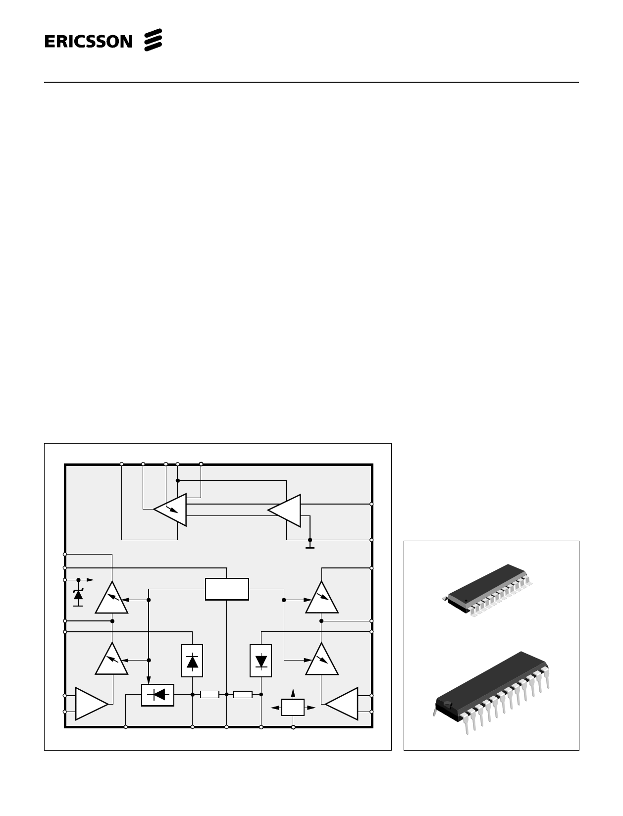
Figure 1. Block diagram.
1
1 page 
PBL 388 14
-Txin 1
+Txin 2
F2out 3
Txout 4
TxDetin 5
TxDetout 6
Ref. 7
N Det 8
CMP 9
RxDetout 10
RxDetin 11
Rxout 12
24 CTR
23 LSPin
22 VA
21 VOL
20 LL
19 LSP
18 GNDA
17 GND
16 V+
15 -Rxin
14 +Rxin
13 F5out
24 pin DIP
Figure 4. Pin configuration.
Pin Descriptions
Refer to figure 6. (24 pin DIP and 24 pin SO package)
Pin Symbol Description
Pin
1
-Txin
Transmitter channel negative input.
11
Input impedance 3.16 kohm.
2
+Txin Transmitter channel positive input.
12
Input impedance 100 kohm.
3
F2out Output of the second amplifier in the
13
transmitter channel.
4
Txout Transmitter channel output. Min. ac
14
load impedance 10 kohm.
5 TxDetin Input of the transmitter channel signal 15
detector. Input impedance 13 kohm.
6 TxDetout Output of the transmitter channel signal 16
detector. Goes nagative referred to the
internal ref. voltage of appx. 2V when a
transmitter signal is present.
17
7 Ref. Internal reference app. 2V.
18
8
NDet
Background noise detector output.
Goes positive referred to the internal ref.
voltage of app. 2V when a background 19
noise signal is present
20
9
CMP
Comparator input. External resistance
to this point should not be less than
21
50 kohm. Summing point to the different
detector outputs.
10
RxDetout Output of the receiver channel signal
22
detector. Goes positive referred to the
internal ref. voltage of appx. 2V when a 23
receiver signal is present
24
-Txin 1
+Txin 2
F2out 3
Txout 4
TxDetin 5
TxDetout 6
Ref. 7
N Det 8
CMP 9
RxDetout 10
RxDetin 11
Rxout 12
24 CTR
23 LSP in
22 VA
21 VOL
20 LL
19 LSP
18 GNDA
17 GND
16 V+
15 -Rxin
14 +Rxin
13 F5out
24 pin SO
Symbol Description
RxDetin
Rxout
F5out
+Rxin
-Rxin
V+
GND
GNDA
LSP
LL
VOL
VA
LSPin
CTR
Input of the receiver channel signal
detector. Input impedance 13 kohm.
Receiver channel output. Min. ac load
impedance 10 kohm.
Output of the second amplifier in the
receiver channel.
Receiver channel positive input. Input
impedance 140 kohm.
Receiver channel negative input. Input
impedance 20 kohm.
Supply of the speech switching circuitry.
A shunt regulator, voltage apprx. 3.3V at
1.0mA.
System ground.
Power amplifier ground. Can lie positive
relative to GND, otherways connected
externally to GND.
Loudspeaker power amplifier output.
Feedback loop input
Volume control input. By sourcing a
current of appx. 0-40 µA into this pin the
gain can be reduced.
Positive supply for the loudspeaker
amplifier.
Loudspeaker amplifier signal input. Input
impedance 30 kohm.
Control input for gain dynamics
(25 or 50dB), mute and disable.
5
5 Page 
PBL 388 14
+
100 µF
6V
15nF
+ 100 µF
16 V
50 Ω
LOUDSPEAKER
+ supply
0V
Tx
signal
68nF
18
24
4
68nF
3
5
16
F3
+
19 21
20 22
PBL 388 14
Control
F6
23
220nF
17
47k
12 100nF
50k
13
68nF
11
820Ω
820Ω
150nF
150nF
1
2 F1
F2
8
F5
1 µF
15
F4 +
Ref.
6 9 10 7
14
33nF
MIC.
6.8nF
470 k
+ 100 µF
6V
+
2.2 µF/6V
+
100nF
2.2 µF/6V
4.7nF
Rx
signal
Figure 18. Application with ac. volume control.
22
PBL
388 14
19
15n
10Ω
20
BD131
15n
BD132
+
+
4 - 15 V
-
+ 1000µF
4Ω
Figure 19. External power amplifier
The power amplifier feedback loop can
be broken (pinns 19 and 20) thus making it
possble to insert external power transistors
to increase the audio output power. This
enables with external power supply an out-
put power of several watts fed into 4 - 16 ohm
loudspeaker. See. fig. 19.
11
11 Page | ||
| Páginas | Total 14 Páginas | |
| PDF Descargar | [ Datasheet PBL388141SO.PDF ] | |
Hoja de datos destacado
| Número de pieza | Descripción | Fabricantes |
| PBL388141SO | Voice - switched 2-channel Circuit with loudspeaker amplifier | Ericsson |
| PBL388141SOT | Voice - switched 2-channel Circuit with loudspeaker amplifier | Ericsson |
| Número de pieza | Descripción | Fabricantes |
| SLA6805M | High Voltage 3 phase Motor Driver IC. |
Sanken |
| SDC1742 | 12- and 14-Bit Hybrid Synchro / Resolver-to-Digital Converters. |
Analog Devices |
|
DataSheet.es es una pagina web que funciona como un repositorio de manuales o hoja de datos de muchos de los productos más populares, |
| DataSheet.es | 2020 | Privacy Policy | Contacto | Buscar |