|
|
|
PDF RF2643 Data sheet ( Hoja de datos )
| Número de pieza | RF2643 | |
| Descripción | 3V DUAL-BAND UPCONVERTER AND DRIVER AMPLIFIER | |
| Fabricantes | RF Micro Devices | |
| Logotipo | ||
Hay una vista previa y un enlace de descarga de RF2643 (archivo pdf) en la parte inferior de esta página. Total 16 Páginas | ||
|
No Preview Available !
Preliminary
6
Typical Applications
• TDMA/AMPS Cellular Systems
• CDMA/AMPS Cellular Systems
RF2643
3V DUAL-BAND UPCONVERTER
AND DRIVER AMPLIFIER
• PCS Systems
• Portable Battery-Powered Equipment
Product Description
The RF2643 is a complete upconverter, dual-power
amplifier driver and attenuator designed for Cellular and
PCS systems. It is designed to upconverter and amplifies
RF signals while providing 22dB of linear gain control
range. It features digital control for the mixer and drivers.
The device features balanced IF inputs, single-ended LO
input and dual RF output for Cellular and PCS Systems
respectively. The IC is manufactured on an advanced Sili-
con Bi-CMOS process and packaged in a 20-pin,
4mmx4mm, leadless chip carrier with an exposed die
flag.
Optimum Technology Matching® Applied
Si BJT
üSi Bi-CMOS
GaAs HBT
SiGe HBT
GaAs MESFET
Si CMOS
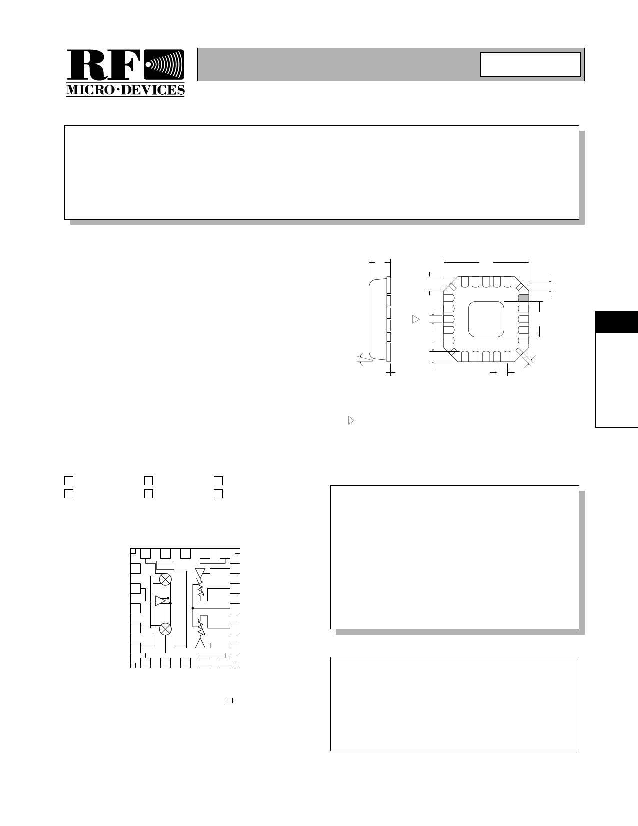
* 20 19 18 17 16 *
PD 1
Logic
15
CELL
ATT GND
LO 2
14 CELL OUT
BYPASS 3
13 VGC
IF+ 4
12 PCS OUT
IF- 5
11
PCS
ATT GND
* 6 7 8 9 10 *
* Represents "GND".
Functional Block Diagram
1.00
0.90
0.60
0.24 typ
3 0.20
4.00
sq.
0.65
0.30
4 PLCS
2.10
sq.
12°
MAX
0.75
0.50
0.05
0.50
Dimensions in mm.
NOTES:
1 Shaded lead is Pin 1.
Note orientation of package.
2 Pin 1 identifier must exist on top surface of package by identification
mark or feature on the package body. Exact shape and size is optional.
3 Dimension applies to plated terminal: to be measured between 0.02 mm
and 0.25 mm from terminal end.
4 Package Warpage: 0.05 mm max.
5 Die Thickness Allowable: 0.305 mm max.
0.23
0.13
4 PLCS
Package Style: LCC, 20-Pin, 4x4
Features
• Single Supply 3.0V Operation
• Power Down Control
• Gain Control Range of 22dB
• Driver Amplifier Select Pin (RF Output
Select)
• High Linearity in Mixer and Driver Amp
Ordering Information
RF2643
3V Dual-Band Upconverter and Driver Amplifier
RF2643 PCBA Fully Assembled Evaluation Board
RF Micro Devices, Inc.
7628 Thorndike Road
Greensboro, NC 27409, USA
Tel (336) 664 1233
Fax (336) 664 0454
http://www.rfmd.com
6
Rev A1 010717
6-37
1 page 
Preliminary
RF2643
Pin
13
14
15
Function
VGC
CELL OUT
CELL
ATT GND
Description
Analog gain control for the driver amplifier. Valid control voltage ranges
from 0.8VDC to 1.9VDC.
Cellular RF output pin. External matching is required. External match-
ing is required. This pin is internally DC biased and should be DC
blocked if it is connected to a device with a DC level present.
Cell attenuator ground pin. This pin should be AC ground. The trace
length between the pin and the bypass capacitors should be minimized.
The value of the capacitor is chosen to resonate in the PCS band.
Interface Schematic
VGC
Cell
Attenuator
CELL OUT
CELL ATT-GND
16 CELL IN Singled end input for the cellular driver and attenuator. External match-
ing is required. This pin is internally DC biased and should be DC
blocked if it is connected to a device with a DC level present.
CELL VCC
17 CELL GND This pin should be choke to ground. The inductor is used to adjust the
linearity of the cellular driver.
18 CELL VCC Supply voltage pin for the cell driver. This pin is an open collector and it
will need a bias choke inductor and RF bypass. A parallel resistor to the
inductor improves stability of the driver amplifier.
19
SEL
Band select control pin for the drivers. When Logic "high" (greater than
2.1V) the PCS band is active. When logic "low" (less than 0.5V) the
Cellular Band is active.
CELL GND
SEL
20
CELL
RF mixer output pin for the PCS system. PCS Mixout output imped-
MIXOUT
ance depends on the LC match and it is influenced by the bypass
capacitor at VCC2.
VCC MIX
Pkg
Base
GND
Ground connection. The backside of the package should be soldered to
a top side ground pad, which is connected to the ground plane. Addi-
tional ground connections are offered at each corner of the package for
flexibility in layout design.
CELL MIXOUT
6
Rev A1 010717
6-41
5 Page 
Preliminary
14.5
14.0
13.5
13.0
12.5
12.0
11.5
11.0
10.5
10.0
2.7
14.0
OIP3, -30º
OIP3, 25º
OIP3, 85º
Cellular Mixer OIP3
@ LO = -10 dBm
2.8 2.9 3.0 3.1
VCC (V)
Cellular Mixer Noise Figure
@ LO = -10 dBm
3.2
3.3
13.5
13.0 NF, -30º
NF, 25º
12.5 NF, 85º
12.0
11.5
11.0
10.5
10.0
2.7 2.8 2.9 3.0 3.1 3.2 3.3
VCC (V)
Cellular Mixer Gain
@ 25°C
0.5
0.0
-0.5
-1.0
-1.5
-2.0
-2.5
-3.0 2.7 V
-3.5 3 V
3.3 V
-4.0
-10.0 -9.0 -8.0 -7.0 -6.0 -5.0 -4.0 -3.0 -2.0
VCC (V)
Rev A1 010717
RF2643
14.5
14.0
13.5
13.0
12.5
12.0
11.5
11.0
10.5
10.0
2.7
13.0
Cellular Mixer OIP3
@ LO = -3 dBm
2.8 2.9 3.0 3.1
VCC (V)
Cellular Mixer Noise Figure
@ LO = -3 dBm
OIP3, -30º
OIP3, 25º
OIP3, 85º
3.2 3.3
6
12.5 NF, -30º
NF, 25º
12.0 NF, 85º
11.5
11.0
10.5
10.0
2.7 2.8 2.9 3.0 3.1 3.2 3.3
VCC (V)
Cellular Mixer OIP3
@ 25°C
14.0
13.5
13.0
12.5
12.0
11.5
11.0
2.7 V
10.5 3 V
3.3 V
10.0
-10.0 -9.0 -8.0 -7.0 -6.0 -5.0 -4.0 -3.0 -2.0
LO (dBm)
6-47
11 Page | ||
| Páginas | Total 16 Páginas | |
| PDF Descargar | [ Datasheet RF2643.PDF ] | |
Hoja de datos destacado
| Número de pieza | Descripción | Fabricantes |
| RF2640 | 3V 900MHZ UPCONVERTER/ DRIVER AMPLIFIER | RF Micro Devices |
| RF2641 | CDMA UPCONVERTER/BPSK MODULATOR | RF Micro Devices |
| RF2642 | 3V 900MHZ UPCONVERTER/ DRIVER AMPLIFIER WITH BYPASS MODE | RF Micro Devices |
| RF2643 | 3V DUAL-BAND UPCONVERTER AND DRIVER AMPLIFIER | RF Micro Devices |
| Número de pieza | Descripción | Fabricantes |
| SLA6805M | High Voltage 3 phase Motor Driver IC. |
Sanken |
| SDC1742 | 12- and 14-Bit Hybrid Synchro / Resolver-to-Digital Converters. |
Analog Devices |
|
DataSheet.es es una pagina web que funciona como un repositorio de manuales o hoja de datos de muchos de los productos más populares, |
| DataSheet.es | 2020 | Privacy Policy | Contacto | Buscar |