|
|
|
PDF UPSD3212 Data sheet ( Hoja de datos )
| Número de pieza | UPSD3212 | |
| Descripción | Flash Programmable System Devices with 8032 Microcontroller Core and 16Kbit SRAM | |
| Fabricantes | STMicroelectronics | |
| Logotipo | ||
Hay una vista previa y un enlace de descarga de UPSD3212 (archivo pdf) en la parte inferior de esta página. Total 30 Páginas | ||
|
No Preview Available !
UPSD3212C
UPSD3212CV
Flash Programmable System Devices
with 8032 Microcontroller Core and 16Kbit SRAM
FEATURES SUMMARY
s The uPSD321X Devices combine a Flash PSD
architecture with an 8032 microcontroller core.
The uPSD321X Devices of Flash PSDs feature
dual banks of Flash memory, SRAM, general
purpose I/O and programmable logic, supervi-
sory functions and access via I2C, ADC and
PWM channels, and an on-board 8032 micro-
controller core, with two UARTs, three 16-bit
Timer/Counters and two External Interrupts. As
with other Flash PSD families, the uPSD321X
Devices are also in-system programmable (ISP)
via a JTAG ISP interface.
s Large 2KByte SRAM with battery back-up
option
s Dual bank Flash memories
– 64KByte main Flash memory
– 16KByte secondary Flash memory
s Content Security
– Block access to Flash memory
s Programmable Decode PLD for flexible address
mapping of all memories within 8032 space.
s High-speed clock standard 8032 core (12-cycle)
s I2C interface for peripheral connections
s 5 Pulse Width Modulator (PWM) channels
s Analog-to-Digital Converter (ADC)
s Six I/O ports with up to 46 I/O pins
s 3000 gate PLD with 16 macrocells
s Supervisor functions with Watchdog Timer
s In-System Programming (ISP) via JTAG
s Zero-Power Technology
s Single Supply Voltage
– 4.5 to 5.5V
– 3.0 to 3.6V
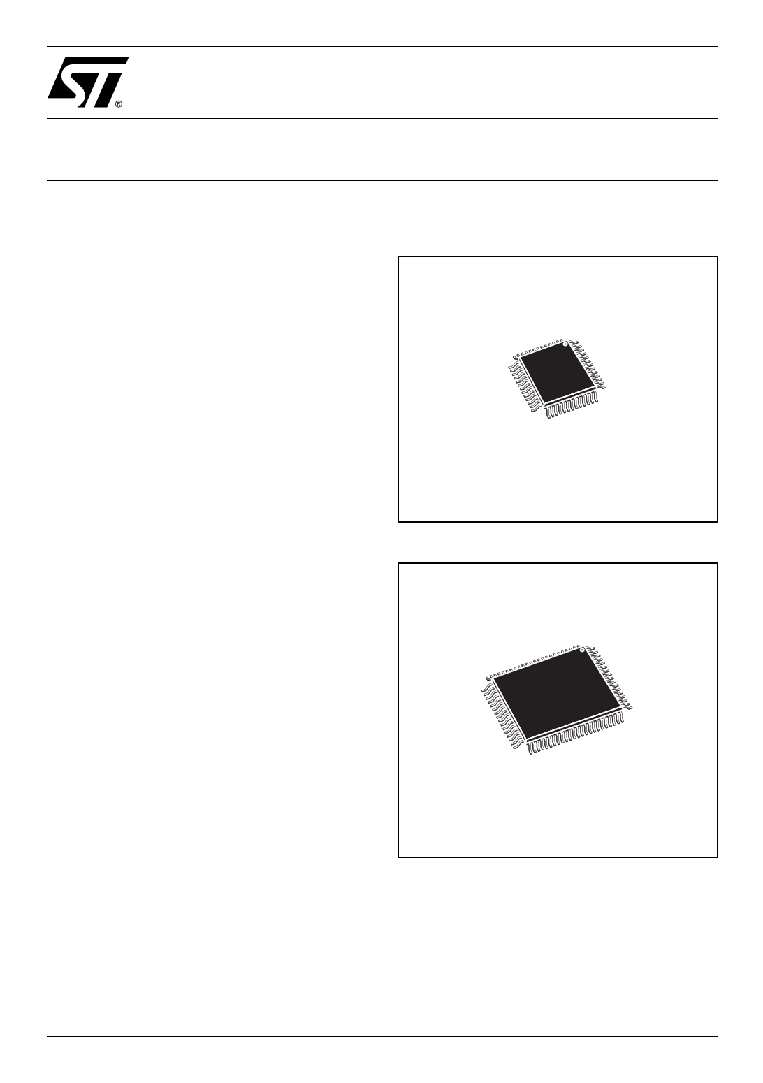
Figure 1. 52-lead, Thin, Quad, Flat Package
TQFP52 (T)
Figure 2. 80-lead, Thin, Quad, Flat Package
TQFP80 (U)
September 2003
Rev. 1.2
1/152
1 page 
UPSD3212C, UPSD3212CV
Timer 2 . . . . . . . . . . . . . . . . . . . . . . . . . . . . . . . . . . . . . . . . . . . . . . . . . . . . . . . . . . . . . . . . . . . . . . 54
Timer/Counter Mode 2: 8-bit Auto-reload (Figure 23.) . . . . . . . . . . . . . . . . . . . . . . . . . . . . . . . . . . 54
Timer/Counter 2 Control Register (T2CON) (Table 40.) . . . . . . . . . . . . . . . . . . . . . . . . . . . . . . . . . 54
Timer/Counter 2 Operating Modes (Table 41.) . . . . . . . . . . . . . . . . . . . . . . . . . . . . . . . . . . . . . . . . 55
Description of the T2CON Bits (Table 42.) . . . . . . . . . . . . . . . . . . . . . . . . . . . . . . . . . . . . . . . . . . . 55
Timer 2 in Capture Mode (Figure 24.) . . . . . . . . . . . . . . . . . . . . . . . . . . . . . . . . . . . . . . . . . . . . . . . 56
Timer 2 in Auto-Reload Mode (Figure 25.) . . . . . . . . . . . . . . . . . . . . . . . . . . . . . . . . . . . . . . . . . . . 56
Timer/Counter Mode 3: Two 8-bit Counters (Figure 26.). . . . . . . . . . . . . . . . . . . . . . . . . . . . . . . . . 57
STANDARD SERIAL INTERFACE (UART) . . . . . . . . . . . . . . . . . . . . . . . . . . . . . . . . . . . . . . . . . . . . . 58
Multiprocessor Communications. . . . . . . . . . . . . . . . . . . . . . . . . . . . . . . . . . . . . . . . . . . . . . . . . 58
Serial Port Control Register . . . . . . . . . . . . . . . . . . . . . . . . . . . . . . . . . . . . . . . . . . . . . . . . . . . . . 59
Serial Port Mode 0, Block Diagram (Figure 27.) . . . . . . . . . . . . . . . . . . . . . . . . . . . . . . . . . . . . . . . 59
Serial Port Control Register (SCON) (Table 43.). . . . . . . . . . . . . . . . . . . . . . . . . . . . . . . . . . . . . . . 59
Description of the SCON Bits (Table 44.) . . . . . . . . . . . . . . . . . . . . . . . . . . . . . . . . . . . . . . . . . . . . 60
Timer 1-Generated Commonly Used Baud Rates (Table 45.) . . . . . . . . . . . . . . . . . . . . . . . . . . . . 62
Serial Port Mode 0, Waveforms (Figure 28.) . . . . . . . . . . . . . . . . . . . . . . . . . . . . . . . . . . . . . . . . . . 63
Serial Port Mode 1, Block Diagram (Figure 29.) . . . . . . . . . . . . . . . . . . . . . . . . . . . . . . . . . . . . . . . 64
Serial Port Mode 1, Waveforms (Figure 30.) . . . . . . . . . . . . . . . . . . . . . . . . . . . . . . . . . . . . . . . . . . 64
Serial Port Mode 2, Block Diagram (Figure 31.) . . . . . . . . . . . . . . . . . . . . . . . . . . . . . . . . . . . . . . . 66
Serial Port Mode 2, Waveforms (Figure 32.) . . . . . . . . . . . . . . . . . . . . . . . . . . . . . . . . . . . . . . . . . . 66
Serial Port Mode 3, Block Diagram (Figure 33.) . . . . . . . . . . . . . . . . . . . . . . . . . . . . . . . . . . . . . . . 67
Serial Port Mode 3, Waveforms (Figure 34.) . . . . . . . . . . . . . . . . . . . . . . . . . . . . . . . . . . . . . . . . . . 67
ANALOG-TO-DIGITAL CONVERTOR (ADC) . . . . . . . . . . . . . . . . . . . . . . . . . . . . . . . . . . . . . . . . . . . 68
ADC Interrupt . . . . . . . . . . . . . . . . . . . . . . . . . . . . . . . . . . . . . . . . . . . . . . . . . . . . . . . . . . . . . . . . . 68
A/D Block Diagram (Figure 35.). . . . . . . . . . . . . . . . . . . . . . . . . . . . . . . . . . . . . . . . . . . . . . . . . . . . 68
ADC SFR Memory Map (Table 46.) . . . . . . . . . . . . . . . . . . . . . . . . . . . . . . . . . . . . . . . . . . . . . . . . 69
Description of the ACON Bits (Table 47.) . . . . . . . . . . . . . . . . . . . . . . . . . . . . . . . . . . . . . . . . . . . . 69
ADC Clock Input (Table 48.) . . . . . . . . . . . . . . . . . . . . . . . . . . . . . . . . . . . . . . . . . . . . . . . . . . . . . . 69
PULSE WIDTH MODULATION (PWM). . . . . . . . . . . . . . . . . . . . . . . . . . . . . . . . . . . . . . . . . . . . . . . . . 70
4-channel PWM Unit (PWM 0-3) . . . . . . . . . . . . . . . . . . . . . . . . . . . . . . . . . . . . . . . . . . . . . . . . . . 70
Four-Channel 8-bit PWM Block Diagram (Figure 36.) . . . . . . . . . . . . . . . . . . . . . . . . . . . . . . . . . . . 71
PWM SFR Memory Map (Table 49.) . . . . . . . . . . . . . . . . . . . . . . . . . . . . . . . . . . . . . . . . . . . . . . . . 72
Programmable Period 8-bit PWM . . . . . . . . . . . . . . . . . . . . . . . . . . . . . . . . . . . . . . . . . . . . . . . . . 73
Programmable PWM 4 Channel Block Diagram (Figure 37.) . . . . . . . . . . . . . . . . . . . . . . . . . . . . . 73
PWM 4 Channel Operation . . . . . . . . . . . . . . . . . . . . . . . . . . . . . . . . . . . . . . . . . . . . . . . . . . . . . . 74
PWM 4 With Programmable Pulse Width and Frequency (Figure 38.) . . . . . . . . . . . . . . . . . . . . . . 74
5/152
5 Page 
UPSD3212C, UPSD3212CV
SUMMARY DESCRIPTION
s Dual bank Flash memories
– Concurrent operation, read from memory
while erasing and writing the other. In-Appli-
cation Programming (IAP) for remote updates
– Large 64KByte main Flash memory for appli-
cation code, operating systems, or bit maps
for graphic user interfaces
– Large 16KByte secondary Flash memory di-
vided in small sectors. Eliminate external EE-
PROM with software EEPROM emulation
– Secondary Flash memory is large enough for
sophisticated communication protocol during
IAP while continuing critical system tasks
s Large SRAM with battery back-up option
– 2KByte SRAM for RTOS, high-level languag-
es, communication buffers, and stacks
s Programmable Decode PLD for flexible address
mapping of all memories
– Place individual Flash and SRAM sectors on
any address boundary
– Built-in page register breaks restrictive 8032
limit of 64KByte address space
– Special register swaps Flash memory seg-
ments between 8032 “program” space and
“data” space for efficient In-Application Pro-
gramming
s High-speed clock standard 8032 core (12-cycle)
– 40MHz operation at 5V, 24MHz at 3.3V
– 2 UARTs with independent baud rate, three
16-bit Timer/Counters and two External Inter-
rupts
s I2C interface for peripheral connections
– Capable of master or slave operation
s 5 Pulse Width Modulator (PWM) channels
– Four 8-bit PWM units
– One 8-bit PWM unit with programmable peri-
od
s 4-channel, 8-bit Analog-to-Digital Converter
(ADC) with analog supply voltage (VREF)
s Six I/O ports with up to 46 I/O pins
– Multifunction I/O: GPIO, I2C, PWM, PLD I/O,
supervisor, and JTAG
– Eliminates need for external latches and logic
s 3000 gate PLD with 16 macrocells
– Create glue logic, state machines, delays,
etc.
– Eliminate external PALs, PLDs, and 74HCxx
– Simple PSDsoft Express software... Free
s Supervisor functions
– Generates reset upon low voltage or watch-
dog time-out. Eliminate external supervisor
device
– RESET Input pin; Reset output via PLD
s In-System Programming (ISP) via JTAG
– Program entire chip in 10 - 25 seconds with
no involvement of 8032
– Allows efficient manufacturing, easy product
testing, and Just-In-Time inventory
– Eliminate sockets and pre-programmed parts
– Program with FlashLINKTM cable and any PC
s Content Security
– Programmable Security Bit blocks access of
device programmers and readers
s Zero-Power Technology
– Memories and PLD automatically reach
standby current between input changes
s Packages
– 52-pin TQFP
– 80-pin TQFP: allows access to 8032 address/
data/control signals for connecting to external
peripherals
11/152
11 Page | ||
| Páginas | Total 30 Páginas | |
| PDF Descargar | [ Datasheet UPSD3212.PDF ] | |
Hoja de datos destacado
| Número de pieza | Descripción | Fabricantes |
| UPSD3212 | Flash Programmable System Devices with 8032 Microcontroller Core and 16Kbit SRAM | STMicroelectronics |
| UPSD3212A | Flash Programmable System Devices | STMicroelectronics |
| UPSD3212C | Flash Programmable System Devices | STMicroelectronics |
| UPSD3212CV | Flash Programmable System Devices | STMicroelectronics |
| Número de pieza | Descripción | Fabricantes |
| SLA6805M | High Voltage 3 phase Motor Driver IC. |
Sanken |
| SDC1742 | 12- and 14-Bit Hybrid Synchro / Resolver-to-Digital Converters. |
Analog Devices |
|
DataSheet.es es una pagina web que funciona como un repositorio de manuales o hoja de datos de muchos de los productos más populares, |
| DataSheet.es | 2020 | Privacy Policy | Contacto | Buscar |