|
|
|
PDF VN770 Data sheet ( Hoja de datos )
| Número de pieza | VN770 | |
| Descripción | QUAD SMART POWER SOLID STATE RELAY FOR COMPLETE H-BRIDGE CONFIGURATIONS | |
| Fabricantes | STMicroelectronics | |
| Logotipo | ||
Hay una vista previa y un enlace de descarga de VN770 (archivo pdf) en la parte inferior de esta página. Total 10 Páginas | ||
|
No Preview Available !
® VN770
QUAD SMART POWER SOLID STATE RELAY
FOR COMPLETE H-BRIDGE CONFIGURATIONS
TYPE
RDS(on) *
IOUT
VN770
0.240 Ω
9A
* Total resistance of one side in bridge configuration
V CC
26 V
s IDEAL AS A LOW VOLTAGE BRIDGE
s VERY LOW STAND-BY POWER
DISSIPATION
s OVER-CURRENT PROTECTED
s STATUS FLAG DIAGNOSTICS ON UPPER
SIDE
s OPEN DRAIN DIAGNOSTICS OUTPUT
s UNDER-VOLTAGE PROTECTION
s SUITABLE AS QUAD SWITCH
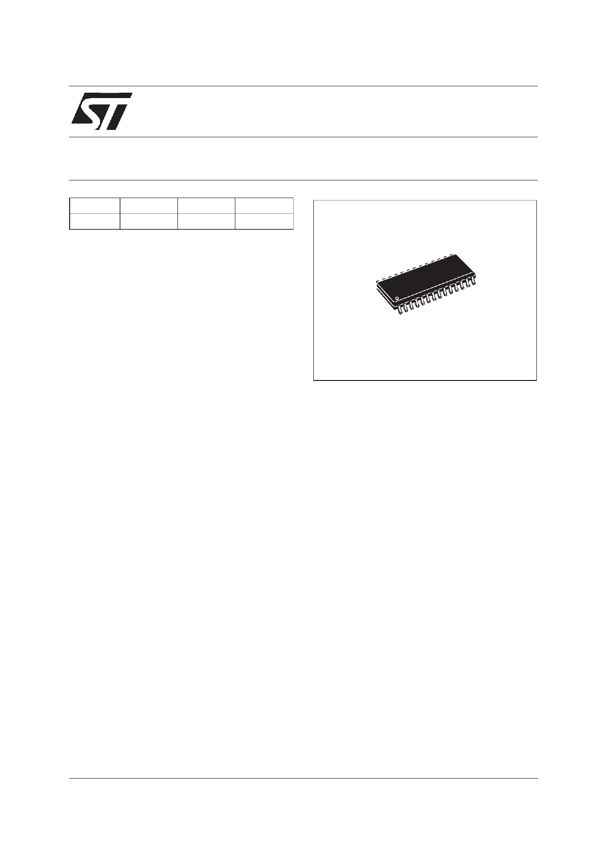
SO-28
DESCRIPTION
The VN770 is a device formed by three
monolithic chips housed in a standard SO-28
package: a double high side and two Power
MOSFETs. The double high side are made using
STMicroelectronics VIPower technology; Power
MOSFETs are made by using the new advanced
strip lay-out technology. This device is suitable to
drive a DC motor in a bridge configuration as well
as to be used as a quad switch for any low
voltage application. The dual high side switches
have built-in thermal shut-down to protect the
chip from over temperature and short circuit,
status output to provide indication for open load
in off and on state, overtemperature conditions
and stuck-on to VCC.
DUAL HIGH-SIDE SWITCH
From the falling edge of the input signal, the
status output, initially low to signal a fault
condition (overtemperature or open load
on-state), will go back to a high state with a
different delay in case of overtemperature (tpovl)
and in case of open open load (tpol) respectively.
This feature allows to discriminate the nature of
the detected fault. To protect the device against
short circuit and over current condition, the
thermal protection turns the integrated Power
MOS off at a minimum junction temperature of
140 oC. When this temperature returns to 125 oC
the switch is automatically turned on again. In
short circuit the protection reacts with virtually no
delay, the sensor (one for each channel) being
located inside each of the two Power MOS areas.
This positioning allows the device to operate with
one channel in automatic thermal cycling and the
other one on a normal load. An internal function
of the devices ensures the fast demagnetization
of inductive loads with a typical voltage (Vdemag)
of -18V. This function allows to greatly reduces
the power dissipation according to the formula:
Pdem = 0.5 • Lload • (Iload)2 • [(VCC+Vdemag)/Vdemag] • f
where f = switching frequency and
Vdemag = demagnetization voltage.
In this device if the GND pin is disconnected, with
VCC not exceeding 16V, both channel will switch
off.
Power MOSFETs
During normal operation, the Input pin is
electrically connected to the gate of the internal
power MOSFET. The devices can be used as a
switch from DC to very high frequency.
October 1998
1/10
1 page 
VN770
LOW SIDE SWITCH
Sy mb o l
Parameter
VDS Drain-Source Voltage (VGS = 0)
VDGR Drain-Gat e Voltage (RGS = 20 KΩ)
VGS Gate-Source Voltage
ID Drain Current (continuous) @ TC = 25 oC
ID Drain Current (continuous) @ TC = 100 oC
IDM(*) Drain Current (pulsed)
dv/dt (1) Peak Diode Recovery Voltage Slope
Ts tg St orage Temperature
Tj Junction Operating Temperature
Value
60
60
±20
36
24
144
7
-55 to 150
-40 to 150
Uni t
V
V
V
A
A
A
V/ ns
oC
oC
THERMAL DATA
Rt hj-ca se
Rt hj-ca se
Rt hj-am b
Thermal Resistance Junction-case (High-side switch)
Thermal Resistance Junction-case (Low-side switch)
Thermal Resistance Junction-ambient
Max
Max
Max
20
20
60
o C /W
o C /W
o C /W
ELECTRICAL CHARACTERISTICS FOR DUAL HIGH SIDE SWITCH
(8 < VCC < 16 V; -40 ≤ Tj ≤ 125 oC unless otherwise specified)
POWER
Sy mb o l
VCC
In(*)
Ro n
IS
VDS(MAX)
Ri
Parameter
Test Conditions
Supply Voltage
Nominal Current
On State Resistance
Tc = 85 oC VDS(o n) ≤ 0. 5 VCC = 13 V
IOUT = In VCC = 13 V Tj = 25 oC
Supply Current
Of f State Tj = 25 oC VCC = 13 V
Maximum Voltage Drop
Output to G ND internal
Im pedance
IOUT = 7.5 A
V
Tj = 25 oC
Tj = 85 oC
VCC = 13
Min.
6
1.6
0.13
1.44
5
Typ .
13
35
10
Max.
26
2.6
0.2
100
2.3
20
Unit
V
A
Ω
µA
V
KΩ
SWITCHING
Sy mb o l
td(on)(^)
tr(^)
td(o ff)( ^)
t f (^ )
(di/dt )on
(di/dt )off
Parameter
Test Conditions
Turn-on Delay Time Of Rout = 5.4 Ω
Output Current
Rise Time Of Output
Current
Rout = 5.4 Ω
Turn-off Delay Time Of Rout = 5.4 Ω
Output Current
Fall Time Of Output
Current
Rout = 5.4 Ω
Turn-on Current Slope Rout = 5.4 Ω
Turn-off Current Slope Rout = 5.4 Ω
Min.
5
Typ .
25
Max.
200
Unit
µs
10 50 180 µs
10 75 250 µs
10 35 180 µs
0.003
0.005
0.1 A/µs
0.1 A/µs
5/10
5 Page | ||
| Páginas | Total 10 Páginas | |
| PDF Descargar | [ Datasheet VN770.PDF ] | |
Hoja de datos destacado
| Número de pieza | Descripción | Fabricantes |
| VN770 | QUAD SMART POWER SOLID STATE RELAY FOR COMPLETE H-BRIDGE CONFIGURATIONS | STMicroelectronics |
| VN770K | QUAD SMART POWER SOLID STATE RELAY FOR COMPLETE H BRIDGE CONFIGURATIONS | ST Microelectronics |
| VN770P | QUAD SMART POWER SOLID STATE RELAY FOR COMPLETE H BRIDGE CONFIGURATIONS | STMicroelectronics |
| VN771 | QUAD SMART POWER SOLID STATE RELAY FOR COMPLETE H-BRIDGE CONFIGURATIONS | STMicroelectronics |
| Número de pieza | Descripción | Fabricantes |
| SLA6805M | High Voltage 3 phase Motor Driver IC. |
Sanken |
| SDC1742 | 12- and 14-Bit Hybrid Synchro / Resolver-to-Digital Converters. |
Analog Devices |
|
DataSheet.es es una pagina web que funciona como un repositorio de manuales o hoja de datos de muchos de los productos más populares, |
| DataSheet.es | 2020 | Privacy Policy | Contacto | Buscar |