|
|
|
PDF ZL50212 Data sheet ( Hoja de datos )
| Número de pieza | ZL50212 | |
| Descripción | 288 Channel Voice Echo Canceller | |
| Fabricantes | Zarlink Semiconductor Inc | |
| Logotipo | ||
Hay una vista previa y un enlace de descarga de ZL50212 (archivo pdf) en la parte inferior de esta página. Total 30 Páginas | ||
|
No Preview Available !
Features
• ZL50212 has nine Echo Voice Processors in a
single BGA package. This single device provides
288 channels of 64 msec echo cancellation or 144
channels at 128 msec echo cancellation
• Each Echo Voice Processor has the capability of
cancelling echo over 32 channels
• Each Echo Voice Processor (EVP) shares the
address bus and data bus with each other
• Fully compliant to ITU-T G.165, G.168 (2000) and
(2002) specifications
• Passed all AT&T voice quality tests for carrier
grade echo canceller
• The ZL50212 provides more than 63% board
space savings when compared with the nine Echo
Voice Processors packaged devices
• Each EVP has a Patented Advanced Non-Linear
Processor with high quality subjective performance
• Each EVP has protection against narrow band
signal divergence and instability in high echo
environments
• Each EVP can be programmed independently in
any mode e.g. Back-to-Back or Extended Delay to
provide capability of cancelling different echo tails.
• Each EVP has 0 to -12 dB level adjusters at all
signal ports (Rin, Sin, Sout and Rout)
• Each EVP has the same JTAG identification code
ZL50212
288 Channel Voice Echo Canceller
Data Sheet
March 2003
Ordering Information
ZL50212GB 535 - Ball BGA
-40°C to +85°C
Applications
• Voice over IP network gateways
• Voice over ATM, Frame Relay
• T1/E1/J1 multichannel echo cancellation
• Wireless base stations
• Echo Canceller pools
• DCME, satellite and multiplexer system
Description
The ZL50212 Voice Echo Canceller implements a cost
effective solution for telephony voice-band echo
cancellation conforming to ITU-T G.168 requirements.
The ZL50212 architecture contains 144 groups of two
echo cancellers (ECA and ECB) which can be
configured to provide two channels of 64 milliseconds
or one channel of 128 milliseconds echo cancellation.
This provides 288 channels of 64 milliseconds to 144
channels of 128 milliseconds echo cancellation or any
combination of the two configurations. The ZL50212
supports ITU-T G.165 and G.164 tone disable
requirements.
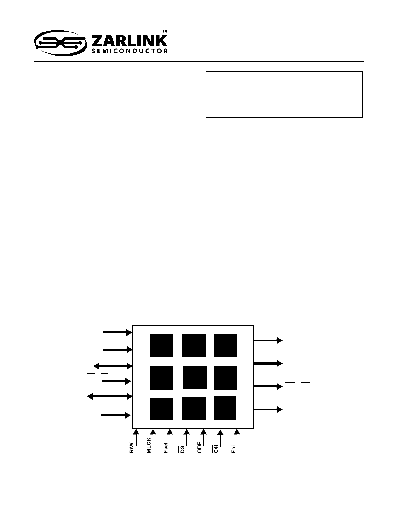
Rin1...Rin9
Sin1....Sin9
D0....D7
CS1..CS9
A0..A12
RESET1..RESET9
ZL50212GB
EVP1 EVP2 EVP3
EVP4 EVP9 EVP5
EVP6 EVP7 EVP8
Rout1..Rout9
Sout1..Sout9
IRQ1..IRQ9
DTA1..DTA9
Figure 1 - ZL50212 Device Overview
1
1 page 
Data Sheet
Pin Description (continued)
Signal
Name
INPUT TEST
PINS
THalt
and TStep
Signal
Type
BGA Ball #
SC_EN,
SC_FCLK,
SC_IN,
SC_M_MCLK,
SC_RESET,
SC_SET,
SC_T_MCLK,
A27,D5,A25,A26,A24,B24,A28
Halt
Step
C14, D14
ZL50212
Signal Description
Internal Connection.
Connected to VSS for
normal operation.
Internal Connection.
Connected to VSS for
normal operation.
Signal Name
Signal
Type
BGA Ball #
Signal Description
USER SIGNAL PINS
D0, D1, D2, D3, D4, D5,
D6, D7
A0,A1,A2,A3,A4,A5,
A6,A7, A8, A9,
A10,A11,A12
CS1,CS2,CS3,
CS4, CS5, CS6,
CS7, CS8, CS9
RESET1 RESET2,
RESET3, RESET4,
RESET5, RESET6,
RESET7, RESET8,
RESET9
Rin1, Rin2, Rin3,
Rin4, Rin5, Rin6,
Rin7, Rin8, Rin9
Sin1, Sin2, Sin3, Sin4,
Sin5, Sin6, Sin7, Sin8,
Sin9
Rout1, Rout2, Rout3,
Rout4, Rout5, Rout6,
Rout7, Rout8, Rout9
User
Signals
User
Signals
User
Signals
User
Signals
User
Signals
User
Signals
User
Signals
AK7,AJ8,AK8, Data Bus D0 to D7 (Bidirectional). These pins form
AJ27,AK29,AJ28, the 8-bit bidirectional data bus of the microprocessor
AH27, AJ30 port. They are connected to all the EVP’s.
AG28,AH29, Address A0 to A12 (Input). These inputs provide the
AH30,AG29,AF28, A12 - A0 address lines to the internal registers. They
AG30,AE28,AF29, are connected to all the EVP’s.
AE29,AF30,AD27,
AE30,AD28
R5,L28,T5,AF15, Chip Select (Input). These active low inputs are used
AF16,E16,T26, to enable the microprocessor interface of each EVP .
R26,E15
EVP Reset (Schmitt Trigger Input). An active low
resets the device and puts the Voice Processor into a
M2,AH23,M1,AH5, low-power stand-by mode. When the RESET pin is
AJ5,AJ23,N29, returned to logic high and a clock is applied to the
M30, AK14 MCLK pin, the EVP will automatically execute
initialization routines, which preset all the Control
and Status Registers to their default power-up
values. Each reset pin controls a single processor. A
user can connect all of them together if required.
C6,V27,B5,AG5, Receive PCM Signal Inputs (Inputs). Port 1 TDM
AH6,U28,B27,B28, data input streams. Each Rin pin receives serial TDM
D13 data streams at 2.048 Mb/s with 32 channels per
stream.
C7,U30,B6,AG7, Send PCM Signal Inputs (Inputs). Port 2 TDM data
AG6,U29,B30,C27, input streams. Each Sin pin receives serial TDM data
A12 streams at 2.048 Mb/s with 32 channels per stream.
A5,V30,A6,AH7, Receive PCM Signal Outputs (Outputs). Port 2 TDM
AG8,V28,C26,C30, data output streams. Each Rout pin outputs serial
C13 TDM data streams at 2.048 Mb/s with 32 channels per
stream.
Zarlink Semiconductor Inc.
5
5 Page 
Data Sheet
2.2 Non-Linear Processor (NLP)
ZL50212
After echo cancellation, there is always a small amount of residual echo which may still be audible. The EVP uses
Zarlink’s patented Advanced NLP to remove residual echo signals which have a level lower than the Adaptive
Suppression Threshold (TSUP in G.168). This threshold depends upon the level of the Rin (Lrin) reference signal as
well as the programmed value of the Non-Linear Processor Threshold register (NLPTHR). TSUP can be calculated
by the following equation:
TSUP = Lrin + 20log10(NLPTHR)
where NLPTHR is the Non-Linear Processor Threshold register value and Lrin is the relative power level expressed
in dBm0. The NLPTHR register is 16 bits wide. The register value in hexadecimal can be calculated with the following
equation:
where 0 < NLPTHR(dec) < 1
NLPTHR(hex) = hex(NLPTHR(dec) * 32768)
When the level of residual error signal falls below TSUP, the NLP is activated further attenuating the residual signal
by an additional 30 dB. To prevent a perceived decrease in background noise due to the activation of the NLP, a
spectrally-shaped comfort noise, equivalent in power level to the background noise, is injected. This keeps the
perceived noise level constant. Consequently, the user does not hear the activation and de-activation of the NLP.
The NLP processor can be disabled by setting the NLPDis bit to “1” in Control Register 2.
The comfort noise injector can be disabled by setting the INJDis bit to “1” in Control Register 1. It should be noted
that the NLPTHR is valid and the comfort noise injection is active only when the NLP is enabled.
The patented Advanced NLP provides a number of new and improved features over the original NLP found in
previous generation devices. The differences between the Advanced NLP and the original NLP are summarized in
Table 1.
Feature
Register or Bit(s)
Advanced
NLP Default
Value
Original NLP
Default Value
NLP Selection
NLPSel (Control Register 3) 1
Reject uncanceled echo as noise
NLRun1 (Control Register 3) 1
Reject double-talk as noise
NLRun2 (Control Register 3) 1
Noise level estimator ramping scheme InjCtrl (Control Register 3)
1
Noise level ramping rate
Noise level scaling
NLInc (Noise Control)
Noise Scaling
5(hex)
16(hex)
0 (feature
not supported)
0 (feature
not supported)
0 (feature
not supported)
0 (feature
not supported)
C(hex)
74(hex)
Table 1 - Comparison of NLP Types
The NLPSel bit in Control Register 3 selects which NLP is used. A “1” will select the Advanced NLP, “0” selects the
original NLP.
The Advanced NLP uses a new noise ramping scheme to quickly and more accurately estimate the background
noise level. The noise ramping method of the original NLP can also be used. The InjCtrl bit in Control Register 3
selects the ramping scheme.
Zarlink Semiconductor Inc.
11
11 Page | ||
| Páginas | Total 30 Páginas | |
| PDF Descargar | [ Datasheet ZL50212.PDF ] | |
Hoja de datos destacado
| Número de pieza | Descripción | Fabricantes |
| ZL50211 | 256 Channel Voice Echo Canceller | Zarlink Semiconductor |
| ZL50212 | 288 Channel Voice Echo Canceller | Zarlink Semiconductor Inc |
| Número de pieza | Descripción | Fabricantes |
| SLA6805M | High Voltage 3 phase Motor Driver IC. |
Sanken |
| SDC1742 | 12- and 14-Bit Hybrid Synchro / Resolver-to-Digital Converters. |
Analog Devices |
|
DataSheet.es es una pagina web que funciona como un repositorio de manuales o hoja de datos de muchos de los productos más populares, |
| DataSheet.es | 2020 | Privacy Policy | Contacto | Buscar |