|
|
|
PDF IRF9540N Data sheet ( Hoja de datos )
| Número de pieza | IRF9540N | |
| Descripción | Power MOSFET(Vdss=-100V/ Rds(on)=0.117ohm/ Id=-23A) | |
| Fabricantes | International Rectifier | |
| Logotipo | ||
1. IRF9540N mosfet datasheet Hay una vista previa y un enlace de descarga de IRF9540N (archivo pdf) en la parte inferior de esta página. Total 8 Páginas | ||
|
No Preview Available !
l Advanced Process Technology
l Dynamic dv/dt Rating
l 175°C Operating Temperature
l Fast Switching
l P-Channel
l Fully Avalanche Rated
Description
Fifth Generation HEXFETs from International Rectifier
utilize advanced processing techniques to achieve
extremely low on-resistance per silicon area. This
benefit, combined with the fast switching speed and
ruggedized device design that HEXFET Power
MOSFETs are well known for, provides the designer
with an extremely efficient and reliable device for use
in a wide variety of applications.
The TO-220 package is universally preferred for all
commercial-industrial applications at power dissipation
levels to approximately 50 watts. The low thermal
resistance and low package cost of the TO-220
contribute to its wide acceptance throughout the
industry.
Absolute Maximum Ratings
ID @ TC = 25°C
ID @ TC = 100°C
IDM
PD @TC = 25°C
VGS
EAS
IAR
EAR
dv/dt
TJ
TSTG
Parameter
Continuous Drain Current, VGS @ -10V
Continuous Drain Current, VGS @ -10V
Pulsed Drain Current
Power Dissipation
Linear Derating Factor
Gate-to-Source Voltage
Single Pulse Avalanche Energy
Avalanche Current
Repetitive Avalanche Energy
Peak Diode Recovery dv/dt
Operating Junction and
Storage Temperature Range
Soldering Temperature, for 10 seconds
Mounting torque, 6-32 or M3 srew
Thermal Resistance
RθJC
RθCS
RθJA
Parameter
Junction-to-Case
Case-to-Sink, Flat, Greased Surface
Junction-to-Ambient
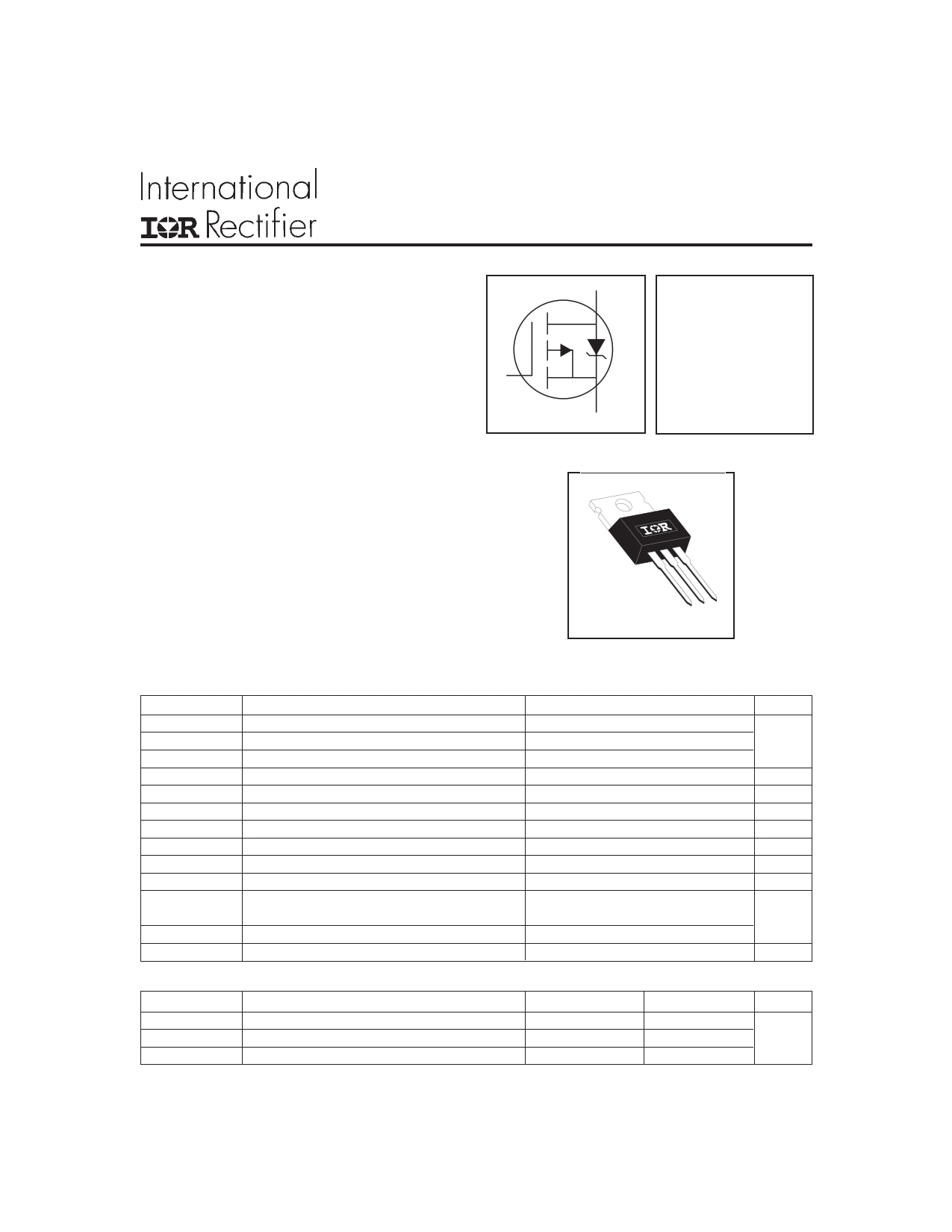
G
PD - 91437B
IRF9540N
HEXFET® Power MOSFET
D
VDSS = -100V
RDS(on) = 0.117Ω
ID = -23A
S
TO-220AB
Max.
-23
-16
-76
140
0.91
± 20
430
-11
14
-5.0
-55 to + 175
300 (1.6mm from case )
10 lbf•in (1.1N•m)
Typ.
–––
0.50
–––
Max.
1.1
–––
62
Units
A
W
W/°C
V
mJ
A
mJ
V/ns
°C
Units
°C/W
5/13/98
1 page 
25
20
15
10
5
0
25 50 75 100 125 150 175
TC , Case Temperature ( °C)
Fig 9. Maximum Drain Current Vs.
Case Temperature
10
IRF9540N
VDS
VGS
RG
RD
D.U.T.
-10V
Pulse Width ≤ 1 µs
Duty Factor ≤ 0.1 %
-
+ VDD
Fig 10a. Switching Time Test Circuit
VGS
10%
td(on) tr
td(off) tf
90%
VDS
Fig 10b. Switching Time Waveforms
1
D = 0.50
0.20
0.10
0.1 0.05
0.02
0.01
0.01
0.00001
PDM
t1
SINGLE PULSE
(THERMAL RESPONSE)
t2
Notes:
1. Duty factor D = t1 / t 2
2. Peak T J = P DM x Z thJC + TC
0.0001
0.001
0.01
t1, Rectangular Pulse Duration (sec)
0.1
Fig 11. Maximum Effective Transient Thermal Impedance, Junction-to-Case
1
5 Page | ||
| Páginas | Total 8 Páginas | |
| PDF Descargar | [ Datasheet IRF9540N.PDF ] | |
Hoja de datos destacado
| Número de pieza | Descripción | Fabricantes |
| IRF9540 | 19A/ 100V/ 0.200 Ohm/ P-Channel Power MOSFETs | Intersil Corporation |
| IRF9540 | Power MOSFET(Vdss=-100V/ Rds(on)=0.117ohm/ Id=-23A) | International Rectifier |
| IRF9540 | (IRF9540 - IRF9543) P-CHANNEL POWER MOSFETS | Harris Corporation |
| IRF9540 | (IRF9540 / IRF9541) P-CHANNEL POWER MOSFETS | Samsung semiconductor |
| Número de pieza | Descripción | Fabricantes |
| SLA6805M | High Voltage 3 phase Motor Driver IC. |
Sanken |
| SDC1742 | 12- and 14-Bit Hybrid Synchro / Resolver-to-Digital Converters. |
Analog Devices |
|
DataSheet.es es una pagina web que funciona como un repositorio de manuales o hoja de datos de muchos de los productos más populares, |
| DataSheet.es | 2020 | Privacy Policy | Contacto | Buscar |