|
|
|
PDF SCANPSC100FSC Data sheet ( Hoja de datos )
| Número de pieza | SCANPSC100FSC | |
| Descripción | Embedded Boundary Scan Controller (IEEE 1149.1 Support) | |
| Fabricantes | Fairchild Semiconductor | |
| Logotipo | ||
Hay una vista previa y un enlace de descarga de SCANPSC100FSC (archivo pdf) en la parte inferior de esta página. Total 21 Páginas | ||
|
No Preview Available !
December 1991
Revised May 2000
SCANPSC100F
Embedded Boundary Scan Controller
(IEEE 1149.1 Support)
General Description
The SCANPSC100F is designed to interface a generic par-
allel processor bus to a serial scan test bus. It is useful in
improving scan throughput when applying serial vectors to
system test circuitry and reduces the software overhead
that is associated with applying serial patterns with a paral-
lel processor. The SCANPSC100F operates by serializing
data from the parallel bus for shifting through the chain of
1149.1 compliant components (i.e., scan chain). Scan data
returning from the scan chain is placed on the parallel port
to be read by the host processor. Up to two scan chains
can be directly controlled with the SCANPSC100F via two
independent TMS pins. Scan control is supplied with user
specific patterns which makes the SCANPSC100F proto-
col-independent. Overflow and underflow conditions are
prevented by stopping the test clock. A 32-bit counter is
used to program the number of TCK cycles required to
complete a scan operation within the boundary scan chain
or to complete a SCANPSC100F Built-In Self Test (BIST)
operation. SCANPSC100F device drivers and 1149.1
embedded test application code are available with Fair-
child’s SCAN Ease software tools.
Features
s Compatible with IEEE Std. 1149.1 (JTAG) Test Access
Port and Boundary Scan Architecture
s Supported by Fairchild’s SCAN Ease (Embedded Appli-
cation Software Enabler) Software
s Uses generic, asynchronous processor interface; com-
patible with a wide range of processors and PCLK fre-
quencies
s Directly supports up to two 1149.1 scan chains
s 16-bit Serial Signature Compaction (SSC) at the Test
Data In (TDI) port
s Automatically produces pseudo-random patterns at the
Test Data Out (TDO) port
s Fabricated on FACT 1.5 µm CMOS process
s Supports 1149.1 test clock (TCK) frequencies up to
25 MHz
s TTL-compatible inputs; full-swing CMOS outputs with
24 mA source/sink capability
Ordering Code:
Order Number Package Number
Package Description
SCANPSC100FSC
M28B
28-Lead Small Outline Integrated Circuit (SOIC), JEDEC MS-013, 0.300 Wide
Devices also available in Tape and Reel. Specify by appending the suffix letter “X” to the ordering code.
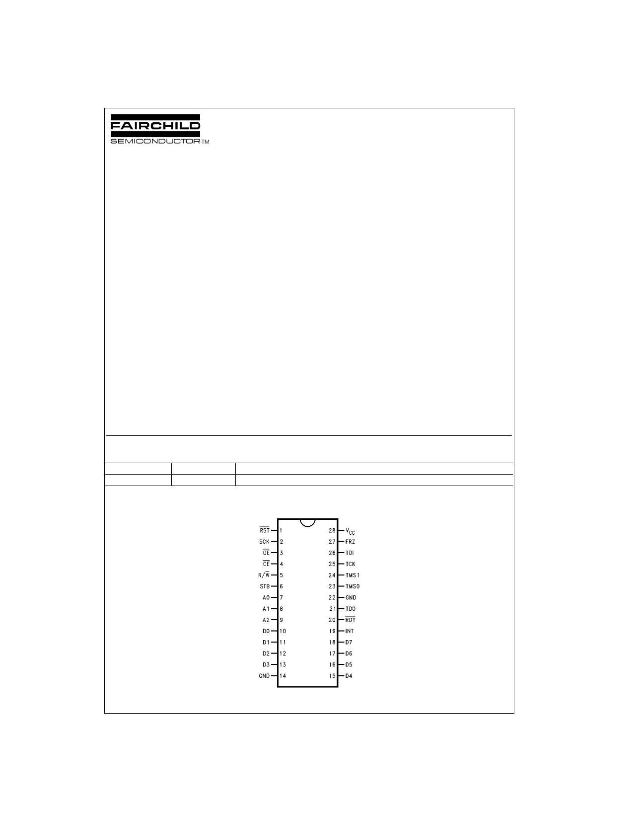
Connection Diagram
FACT is a trademark of Fairchild Semiconductor Corporation.
© 2000 Fairchild Semiconductor Corporation DS010968
www.fairchildsemi.com
1 page 
Mode and Status Registers (Continued)
MODE REGISTER 2 (MODE2)
Write:
Bit 7
Not
Used
Bit 6
Not
Used
Bit 5
Not
Used
Bit 4
Not
Used
Read:
Bit 7
TDO
Status
Bit 6
TDI
Status
Bit 5
CNT32
Status
Bit 4
TMS0
Status
This register contains both mode and status bits. Bits 4–7
are status bits only. Bit 3 is a status bit during read opera-
tions and a mode bit during write operations. Bits 0–2 are
mode bits only. Upon RST low, or a synchronous reset, the
value placed in MODE2 is 10111000 (Read mode). Latches
used to update status bits 3–7 retain their last state upon
RST and are in an “unknown” state after power-up. To ini-
tialize the latches to a known state, they need to be
updated using the Update Status bit (bit 2) or continuous
update bit (bit 3).
• Bit 7:
Set high if the TDO shifter/buffer is not full,
i.e., one or both 8-bit TDO FIFOs are ready to
be written to.
• Bit 6:
Set high if the TDI shifter/buffer is not empty,
i.e., one or both 8-bit TDI FIFOs are ready to
be read from.
• Bit 5:
Set high if the 32-bit counter has not been
loaded, or has reached terminal count.
• Bit 4:
Set high if the TMS0 shifter/buffer is not full,
i.e., one or both 8-bit TMS0 FIFOs are ready
to be written to.
• Bit 3
(Read Cycle):
Set high if the TMS1 shifter/buffer is not full,
i.e., one or both 8-bit TMS1 FIFOs are ready
to be written to.
• Bit 3
(Write Cycle):
If set, will cause all status bits to be continu-
ously updated.
• Bit 2
(Read Cycle):
Shows the state of the Continuous Update bit
during read operations (Bit 3 during writes).
• Bit 2
(Write Cycle):
If set, will cause a pulse to be issued internally
that will update all status bits. This bit will be
reset upon completion of the pulse. The state
of this bit is not readable. It is reset upon RST
low.
• Bit 1:
If set, will cause a synchronous reset of all
functions except the parallel interface. The
value of this bit will return to zero when the
reset operation is complete.
• Bit 0:
If set, will cause the 32-bit counter to count for
one SCK cycle (no TCK cycle will be gener-
ated). The value of this bit will return to zero
when the single step operation is complete.
Bit 3
Continuous
Update
Bit 2
Update
Status
Bit 1
Reset
Bit 0
Single
Step
CNT32
Bit 3
TMS1
Status
Bit 2
Continuous
Update
Bit 1
Reset
Bit 0
Single
Step
CNT32
PROGRAMMING RESTRICTIONS
Because certain mode bits enable shift operations for cer-
tain functions, these mode bits should not be changed
when shift operations are in progress. The alignment of all
registers during shift operations is controlled by a 3-bit
counter in the TCK control block. Enabling or disabling a
function in the middle of a shift operation may disrupt the
logic necessary to keep all shifter/buffers byte-aligned.
For example, if the TDO shifter/buffer (already loaded) is
enabled while the 3-bit counter value is 3, the shifter/buffer
will only shift out only five bits of the first byte loaded.
The following bits should not be changed when shift opera-
tions are in progress, i.e., when TCK is enabled (see sec-
tion on TCK Control).
• MODE0(7:3)
• MODE1(4:3)
• MODE2(0)
Parallel Processor Interface (PPI)
ADDRESS ASSIGNMENT
The following table defines which register is selected for
access with the address lines, A(2:0).
A2 A1 A0 R/W
Function
000
0 TDO Shifter/Buffer
000
1 Counter Register 1
001
0 TDI Shifter/Buffer
001
1 TDI Shifter/Buffer
010
0 TMS0 Shifter/Buffer
010
1 Counter Register 2
011
0 TMS1 Shifter/Buffer
011
1 Counter Register 3
100
0 32-Bit Counter
100
1 Counter Register 0
101
0 MODE0
101
1 MODE0
110
0 MODE1
110
1 MODE1
111
0 MODE2
111
1 MODE2
5 www.fairchildsemi.com
5 Page 
Serial Scan Interface (SSI) (Continued)
TMS(1:0) SHIFTER/BUFFERS
The TMS Shifter/Buffer block diagram is shown in Figure
10. These two blocks take parallel data and serialize it for
shift operations through the serial port pins TMS0 and
TMS1.
Double-buffering is achieved by configuring the shifter/
buffer as a 2 x 8 FIFO. Write and shift operations are con-
trolled by a local state machine that accepts stimulus from
the PPI, Mode Registers, CNT32 and TCK Control section.
The TMS outputs always change on the falling edge of
SCK. The order of shifting is least significant bit first.
TMS(1:0) are forced HIGH upon RST LOW. TMS(1:0) are
3-STATEd when OE is HIGH.
Write operations are completed if the shifter/buffer is not
full (independent of whether shifter/buffer is enabled or dis-
abled). Otherwise they are ignored. Shifting occurs when
the following conditions are all true:
• TMS is enabled with its respective mode bit.
• TMS shifter/buffer is not empty.
• TCK is enabled according to the logic in TCK Control.
When shift operations are not enabled, the TMS output
retains its last state. During long shift sequences, the TMS
shifter/buffer can be disabled and held static so that shift
operations are concentrated only on TDI and TDO. The
TMS output also retains its last state when Test Loop-Back
operations are in progress.
Local select circuitry is used to toggle back and forth
between the two registers of the “FIFO” when shifting. At
any given time, one register is selected for shift operations.
The other holds its previous state or can accept new paral-
lel data. Shift register selection changes due to the follow-
ing two events:
• CNT3 in TCK Control signals that 8 bits have been
shifted. This event is used for basic toggling between
each of the two shift registers.
• CNT32 enabled and at terminal count. This event is
used to account for scan lengths which are not multiples
of eight. When shift register selection changes due to
this signal, any data remaining in the shift register is
unused.
AUTO TMS HIGH MODE. This feature is included in the
TMS shifter/buffer block to improve the efficiency of the
PSC100 in supporting shift operations within the 1149.1
devices connected to the SSI. Shifting data and instruc-
tions into 1149.1 compliant devices requires that their TAP
controllers be sequenced to the Shift-DR or Shift-IR states
(see Figure 8). Once in this state, shifting occurs by holding
TMS LOW and clocking TCK. The last bit is shifted when
the TAP controller transitions to the EXIT1 state. This tran-
sition requires a logic 1 on TMS. The Auto TMS High fea-
ture, enabled by setting bit 1 of Mode Register 0,
automatically creates a logic 1 on the TMS lines of the
PSC100 when CNT32 = 1. Consequently, the last bit is
shifted out without having to load specific TMS data into
the shifter/buffer.
Note: Auto TMS High mode creates a logic 1 on both TMS lines (i.e., TMS0
and TMS1). Therefore, when using the Auto TMS High feature, all 1149.1
devices connected to the TMS line not participating in the current JTAG test
operations should be placed in the Test-Logic-Reset TAP controller state to
prevent inadvertent TAP controller transitions.
TDO SHIFTER/BUFFER
The TDO Shifter/Buffer block diagram is shown in Figure
11. This block takes parallel data and serializes it for shift
operations through the serial port pin TDO. During normal
shift modes, double-buffering is achieved by configuring
the shifter/buffer as a 2 x 8 FIFO. This block can also be
configured as a 32-bit Pseudo Random Pattern Generator
(PRPG) with two additional 8-bit parallel-to-serial shift reg-
isters. Write and shift operations are controlled by a local
state machine that accepts stimulus from the PPI, Mode
Registers, CNT32, and the TCK Control section. The TDO
output always changes on the falling edge of SCK. The
order of shifting is least significant bit first. TDO is forced
high upon RST LOW. TDO is 3-STATEd when OE is HIGH.
Write operations are completed if the shifter/buffer is not
full (independent of whether shifter/buffer is enabled or dis-
abled). Otherwise they are ignored.
Shifting occurs when the following conditions are all true:
• TDO is enabled with its respective mode bit.
• TDO shifter/buffer is not empty.
• TCK is enabled according to the logic in TCK Control.
When shift operations are not enabled, the TDO output
retains its last state. The TDO output also retains its last
state when Test Loop-Back operations are in progress.
Local select circuitry is used to toggle back and forth
between the two registers of the “FIFO” when shifting. At
any given time, one register is selected for shift operations.
The other holds its previous state or can accept new paral-
lel data. Shift register selection changes due to the follow-
ing two events:
• CNT3 in TCK Control signals that 8 bits have been
shifted. This event is used for basic toggling between
each of the two shift registers.
• CNT32 enabled and at terminal count. This event is
used to account for scan lengths which are not multiples
of eight. When shift register selection changes due to
this signal, any data remaining in the shift register is
unused.
PRPG MODE. By setting MODE1(4), the TDO Shifter/
Buffer is reconfigured as a 32-bit PRPG (Pseudo Random
Pattern Generator) using the primitive polynomial:
F(X) = X32 + X22 + X2 + X + 1
The PSC100 was developed to support both 1149.1 and
non-1149.1 serial test methodologies. Since 1149.1 compli-
ant devices include boundary scan registers on control pins
(i.e. OE), which must remain fixed during boundary scan
interconnect testing, generating pseudo-random patterns
with PRPG mode provides limited usefulness for boundary
scan test operations. PRPG mode may provide usefulness
in other serial test or non-test related implementations
which do not require fixed bits in the serial chain.
Figure 12 shows a block diagram of the Linear Feedback
Shift Register hookup.
11 www.fairchildsemi.com
11 Page | ||
| Páginas | Total 21 Páginas | |
| PDF Descargar | [ Datasheet SCANPSC100FSC.PDF ] | |
Hoja de datos destacado
| Número de pieza | Descripción | Fabricantes |
| SCANPSC100FSC | Embedded Boundary Scan Controller (IEEE 1149.1 Support) | Fairchild Semiconductor |
| Número de pieza | Descripción | Fabricantes |
| SLA6805M | High Voltage 3 phase Motor Driver IC. |
Sanken |
| SDC1742 | 12- and 14-Bit Hybrid Synchro / Resolver-to-Digital Converters. |
Analog Devices |
|
DataSheet.es es una pagina web que funciona como un repositorio de manuales o hoja de datos de muchos de los productos más populares, |
| DataSheet.es | 2020 | Privacy Policy | Contacto | Buscar |