|
|
|
PDF K4S161622D Data sheet ( Hoja de datos )
| Número de pieza | K4S161622D | |
| Descripción | 512K x 16Bit x 2 Banks Synchronous DRAM | |
| Fabricantes | Samsung semiconductor | |
| Logotipo | ||
Hay una vista previa y un enlace de descarga de K4S161622D (archivo pdf) en la parte inferior de esta página. Total 30 Páginas | ||
|
No Preview Available !
K4S161622D
512K x 16Bit x 2 Banks Synchronous DRAM
CMOS SDRAM
FEATURES
• 3.3V power supply
• LVTTL compatible with multiplexed address
• Dual banks operation
• MRS cycle with address key programs
-. CAS Latency ( 2 & 3)
-. Burst Length (1, 2, 4, 8 & full page)
-. Burst Type (Sequential & Interleave)
• All inputs are sampled at the positive going edge of the system
clock
• Burst Read Single-bit Write operation
• DQM for masking
• Auto & self refresh
• 15.6us refresh duty cycle (2K/32ms)
GENERAL DESCRIPTION
The K4S161622D is 16,777,216 bits synchronous high data
rate Dynamic RAM organized as 2 x 524,288 words by 16 bits,
fabricated with SAMSUNG′s high performance CMOS technol-
ogy. Synchronous design allows precise cycle control with the
use of system clock I/O transactions are possible on every clock
cycle. Range of operating frequencies, programmable burst
length and programmable latencies allow the same device to be
useful for a variety of high bandwidth, high performance mem-
ory system applications.
ORDERING INFORMATION
Part NO.
K4S161622D-TC/L55
K4S161622D-TC/L60
K4S161622D-TC/L70
K4S161622D-TC/L80
K4S161622D-TC/L10
MAX Freq.
183MHz
166MHz
143MHz
125MHz
100MHz
Interface Package
LVTTL
50
TSOP(II)
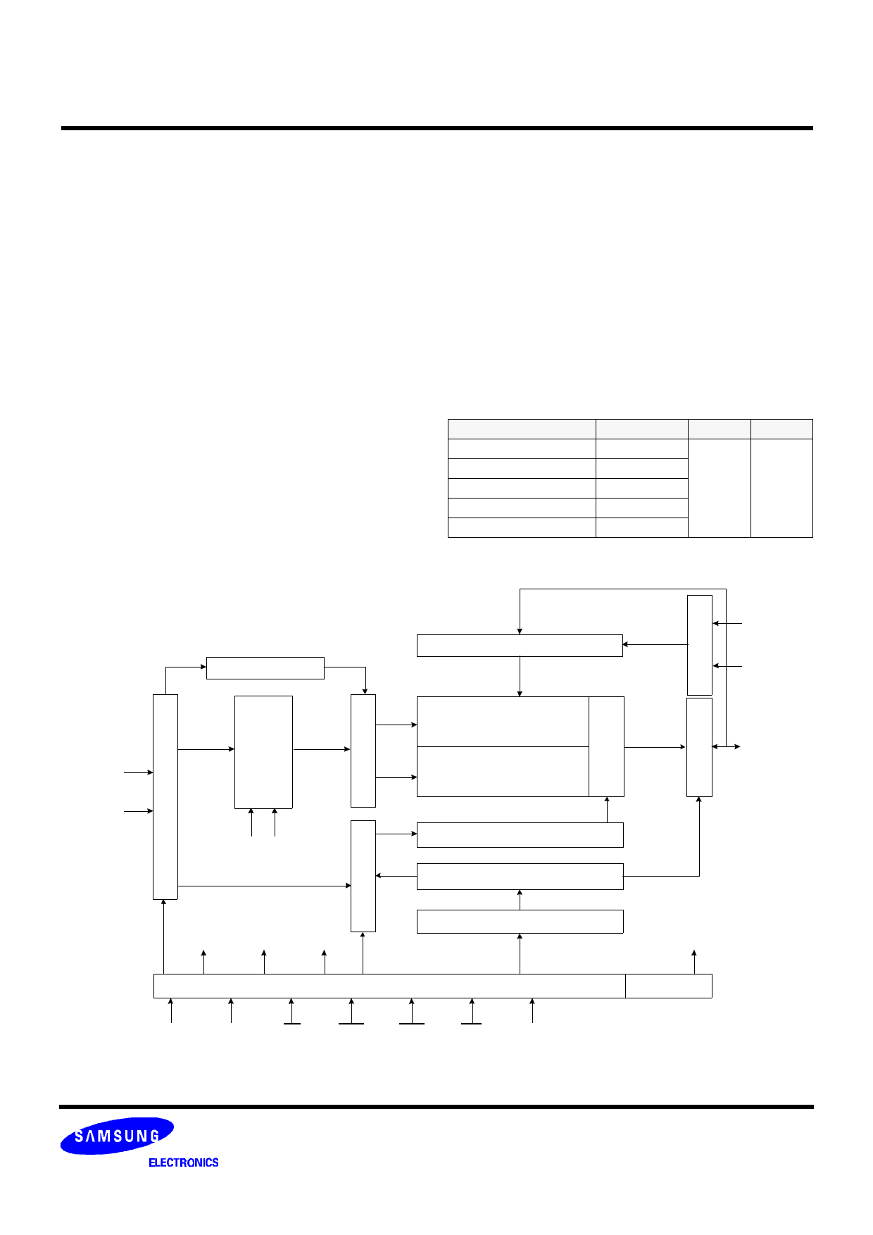
FUNCTIONAL BLOCK DIAGRAM
Bank Select
Data Input Register
LWE
LDQM
512K x 16
CLK
ADD
512K x 16
Column Decoder
LCKE
LRAS LCBR
LWE
LCAS
Latency & Burst Length
Programming Register
LWCBR
Timing Register
DQi
LDQM
CLK CKE
CS
RAS
CAS
WE L(U)DQM
* Samsung Electronics reserves the right to
change products or specification without
notice.
1 page 
K4S161622D
AC OPERATING TEST CONDITIONS (VDD = 3.3V±0.3V*2, TA = 0 to 70°C)
Parameter
Input levels (Vih/Vil)
Input timing measurement reference level
Input rise and fall time
Output timing measurement reference level
Output load condition
Value
2.4 / 0.4
1.4
tr / tf = 1 / 1
1.4
See Fig. 2
3.3V
Output
870Ω
1200Ω
50pF*2
VOH (DC) = 2.4V, IOH = -2mA
VOL (DC) = 0.4V, IOL = 2mA
Output
CMOS SDRAM
Z0=50Ω
Unit
V
V
ns
V
Vtt=1.4V
50Ω
50pF*1
(Fig. 1) DC Output Load Circuit
Note : 1. The DC/AC Test Output Load of K4S161622D-55/60/70 is 30pF.
2. The VDD condition of K4S161622D-55/60 is 3.135V~3.6V.
(Fig. 2) AC Output Load Circuit
OPERATING AC PARAMETER
(AC operating conditions unless otherwise noted)
Parameter
Symbol
CAS Latency
CL
CLK cycle time
tCC(min)
Row active to row active delay
RAS to CAS delay
tRRD(min)
tRCD(min)
Row precharge time
tRP(min)
Row active time
tRAS(min)
tRAS(max)
Row cycle time
tRC(min)
Last data in to row precharge
tRDL(min)
Last data in to new col.address delay
tCDL(min)
Last data in to burst stop
tBDL(min)
Col. address to col. address delay
tCCD(min)
Mode Register Set cycle time
tMRS(min)
Number of valid output data
CAS Latency=3
CAS Latency=2
-55
32
5.5 -
3-
3-
7-
10 -
-60
32
6-
3-
3-
7-
10 -
Version
-70
32
7 8.7
2
32
32
75
100
10 7
1
1
1
1
2
2
1
-80
32
8 10
-10
32
10 12
3 2 22
3 2 22
6 5 54
9 7 76
Unit
CLK
ns
CLK
CLK
CLK
CLK
us
CLK
CLK
CLK
CLK
CLK
CLK
ea
Note
1
1
1
1
1
2, 5
2
2
4
Notes : 1. The minimum number of clock cycles is determined by dividing the minimum time required with clock cycle time and then
rounding off to the next higher integer. Refer to the following clock unit based AC conversion table
5 Page 
K4S161622D
CMOS SDRAM
DEVICE OPERATIONS (Continued)
MODE REGISTER SET (MRS)
The mode register stores the data for controlling the various
operating modes of SDRAM. It programs the CAS latency, burst
type, burst length, test mode and various vendor specific options
to make SDRAM useful for variety of different applications. The
default value of the mode register is not defined, therefore the
mode register must be written after power up to operate the
SDRAM. The mode register is written by asserting low on CS,
RAS, CAS and WE (The SDRAM should be in active mode with
CKE already high prior to writing the mode register). The state of
address pins A0 ~ A10/AP and BA in the same cycle as CS,
RAS, CAS and WE going low is the data written in the mode
register. Two clock cycles is required to complete the write in the
mode register. The mode register contents can be changed
using the same command and clock cycle requirements during
operation as long as all banks are in the idle state. The mode
register is divided into various fields depending on the fields of
functions. The burst length field uses A0 ~ A2, burst type uses
A3, CAS latency (read latency from column address) uses A4 ~
A6, vendor specific options or test mode use A7 ~ A8, A10/AP
and BA. The write burst length is programmed using A9. A7 ~ A8,
A10/AP, BA must be set to low for normal SDRAM operation.
Refer to the table for specific codes for various burst length,
burst type and CAS latencies.
BANK ACTIVATE
The bank activate command is used to select a random row in
an idle bank. By asserting low on RAS and CS with desired row
and bank address, a row access is initiated. The read or write
operation can occur after a time delay of tRCD(min) from the time
of bank activation. tRCD is an internal timing parameter of
SDRAM, therefore it is dependent on operating clock frequency.
The minimum number of clock cycles required between bank
activate and read or write command should be calculated by
dividing tRCD(min) with cycle time of the clock and then rounding
off the result to the next higher integer. The SDRAM has two
internal banks in the same chip and shares part of the internal
circuitry to reduce chip area, therefore it restricts the activation
of two banks simultaneously. Also the noise generated during
sensing of each bank of SDRAM is high, requiring some time for
power supplies to recover before the other bank can be sensed
reliably. tRRD(min) specifies the minimum time required between
activating different bank. The number of clock cycles required
between different bank activation must be calculated similar to
tRCD specification. The minimum time required for the bank to be
active to initiate sensing and restoring the complete row of
dynamic cells is determined by tRAS(min). Every SDRAM bank
activate command must satisfy tRAS(min) specification before a
precharge command to that active bank can be asserted. The
maximum time any bank can be in the active state is determined
by tRAS(max). The number of cycles for both tRAS(min) and
tRAS(max) can be calculated similar to tRCD specification.
BURST READ
The burst read command is used to access burst of data on con-
secutive clock cycles from an active row in an active bank. The
burst read command is issued by asserting low on CS and CAS
with WE being high on the positive edge of the clock. The bank
must be active for at least tRCD(min) before the burst read com-
mand is issued. The first output appears in CAS latency number
of clock cycles after the issue of burst read command. The burst
length, burst sequence and latency from the burst read com-
mand is determined by the mode register which is already pro-
grammed. The burst read can be initiated on any column
address of the active row. The address wraps around if the initial
address does not start from a boundary such that number of out-
puts from each I/O are equal to the burst length programmed in
the mode register. The output goes into high-impedance at the
end of the burst, unless a new burst read was initiated to keep
the data output gapless. The burst read can be terminated by
issuing another burst read or burst write in the same bank or the
other active bank or a precharge command to the same bank.
The burst stop command is valid at every page burst length.
BURST WRITE
The burst write command is similar to burst read command and
is used to write data into the SDRAM on consecutive clock
cycles in adjacent addresses depending on burst length and
burst sequence. By asserting low on CS, CAS and WE with valid
column address, a write burst is initiated. The data inputs are
provided for the initial address in the same clock cycle as the
burst write command. The input buffer is deselected at the end
of the burst length, even though the internal writing can be com-
pleted yet. The writing can be completed by issuing a burst read
and DQM for blocking data inputs or burst write in the same or
another active bank. The burst stop command is valid at every
burst length. The write burst can also be terminated by using
DQM for blocking data and procreating the bank tRDL after the
last data input to be written into the active row. See DQM
OPERATION also.
11 Page | ||
| Páginas | Total 30 Páginas | |
| PDF Descargar | [ Datasheet K4S161622D.PDF ] | |
Hoja de datos destacado
| Número de pieza | Descripción | Fabricantes |
| K4S161622D | 512K x 16Bit x 2 Banks Synchronous DRAM | Samsung semiconductor |
| K4S161622E | 1M x 16 SDRAM | Samsung semiconductor |
| K4S161622E-TC10 | 1M x 16 SDRAM | Samsung semiconductor |
| K4S161622E-TC55 | 1M x 16 SDRAM | Samsung semiconductor |
| Número de pieza | Descripción | Fabricantes |
| SLA6805M | High Voltage 3 phase Motor Driver IC. |
Sanken |
| SDC1742 | 12- and 14-Bit Hybrid Synchro / Resolver-to-Digital Converters. |
Analog Devices |
|
DataSheet.es es una pagina web que funciona como un repositorio de manuales o hoja de datos de muchos de los productos más populares, |
| DataSheet.es | 2020 | Privacy Policy | Contacto | Buscar |