|
|
PDF KM418RD Data sheet ( Hoja de datos )
| Número de pieza | KM418RD | |
| Descripción | 128/144Mbit RDRAM 256K x 16/18 bit x 2*16 Dependent Banks Direct RDRAMTM | |
| Fabricantes | Samsung semiconductor | |
| Logotipo | ||
Hay una vista previa y un enlace de descarga de KM418RD (archivo pdf) en la parte inferior de esta página. Total 30 Páginas | ||
|
No Preview Available !
KM416RD8AC(D)/KM418RD8AC(D)
Direct RDRAM™
128/144Mbit RDRAM
256K x 16/18 bit x 2*16 Dependent Banks
Direct RDRAMTM
Revision 1.01
October 1999
Page -2
Rev. 1.01 Oct. 1999
1 page 
KM416RD8AC(D)/KM418RD8AC(D)
Direct RDRAM™
Pinouts and Definitions
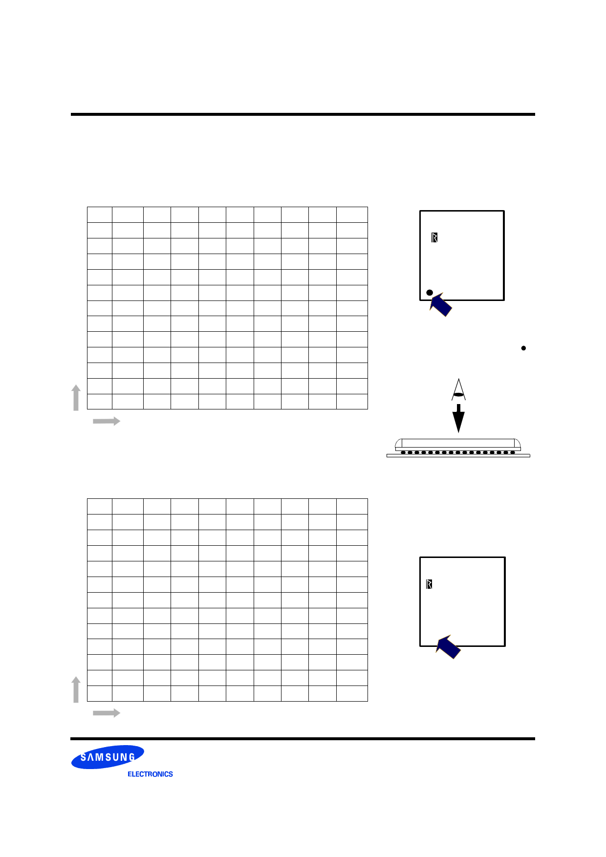
Normal Package
This table shows the pin assignments of the normal RDRAM package.
Table 1 : a. Center-Bonded Device(Top View For Normal Package)
12 GND
11
10 DQA7
9 GND
8 CMD
7
6
5 SCK
4 VCMOS
3 DQA8*
2
1 GND
ROW
A
COL
DQA4
VDD
DQA5
DQA6
GND
DQA3
B
VDD
CFM CFMN
GND GNDa
DQA2 VDDa
DQA1 VREF
VDD
GND
DQA0 CTMN
VDD
CD
RQ5
VDD
RQ6
RQ7
GND
CTM
E
VDD
GND
RQ3
GND
RQ2
DQB0
VDD
DQB1
DQB4
VDD
DQB5
DQB7
GND
SIO1
RQ1
VDD
RQ4
DQB2
GND
RQ0
DQB6
GND
DQB3
SIO0
VCMOS
DQB8*
VDD
GND
F GH
J
b. Top marking example of normal package
SEC KOREA
KM4xxRD8AC
For normal package, pin #1(ROW 1, COL A) is
located at the A1 position on the top side and
the A1 position is marked by the marker “ “.
Top View
Mirrored Package
Chip
This table shows the pin assignments of the mirrored RDRAM package.
Table 2: a.Center-Bonded Device(Top View For Mirrored Package)
12 GND
VDD
VDD
GND
* DQA8/DQB8 are just used for
144Mb RDRAM. These two pins are
NC(No Connection) in 128Mb RDRAM.
11
10
DQA8*
DQA3 DQA0 CTMN
CTM
RQ4
RQ0 DQB3 DQB8* b. Top marking example of mirrored package
9 VCMOS GND VDD GND GND VDD GND GND VCMOS
8
SCK
DQA6 DQA1 VREF
RQ7
RQ1
DQB2 DQB6
SIO0
7 SEC KOREA
6 KM4xxRD8AD
5
CMD
DQA5 DQA2 VDDa
RQ6
RQ2
DQB1 DQB5
SIO1
4
GND
VDD
GND GNDa VDD
GND
VDD
VDD
GND
3
DQA7
DQA4
CFM
CFMN
RQ5
RQ3
DQB0 DQB4
DQB7
M
2
1 GND
VDD
VDD GND For mirrored package, pin #1(ROW 1, COL A)
is located at the A1 postion on the top side and
ROW
A BCDE FGH J
the A1 position is marked by the alphabet “M“.
COL
Page 2 Rev. 1.01 Oct. 1999
5 Page 
KM416RD8AC(D)/KM418RD8AC(D)
Direct RDRAM™
Field Encoding Summary
Table 6 shows how the six device address bits are decoded
for the ROWA and ROWR packets. The DR4T and DR4F
encoding merges a fifth device bit with a framing bit. When
neither bit is asserted, the device is not selected. Note that a
broadcast operation is indicated when both bits are set.
Broadcast operation would typically be used for refresh and
power management commands. If the device is selected, the
DM (DeviceMatch) signal is asserted and an ACT or ROP
command is performed.
Table 6: Device Field Encodings for ROWA Packet and ROWR Packet
DR4T
1
0
1
0
DR4F
1
1
0
0
Device Selection
All devices (broadcast)
One device selected
One device selected
No packet present
Device Match signal (DM)
DM is set to 1
DM is set to 1 if {DEVID4..DEVID0} == {0,DR3..DR0} else DM is set to 0
DM is set to 1 if {DEVID4..DEVID0} == {1,DR3..DR0} else DM is set to 0
DM is set to 0
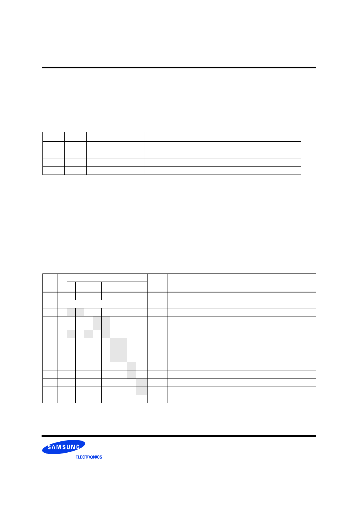
Table 7 shows the encodings of the remaining fields of the
ROWA and ROWR packets. An ROWA packet is specified
by asserting the AV bit. This causes the specified row of the
specified bank of this device to be loaded into the associated
sense amps.
An ROWR packet is specified when AV is not asserted. An
11 bit opcode field encodes a command for one of the banks
of this device. The PRER command causes a bank and its
two associated sense amps to precharge, so another row or
an adjacent bank may be activated. The REFA (refresh-acti-
vate) command is similar to the ACT command, except the
row address comes from an internal register REFR, and
REFR is incremented at the largest bank address. The REFP
(refresh-precharge) command is identical to a PRER
command.
The NAPR, NAPRC, PDNR, ATTN, and RLXR commands
are used for managing the power dissipation of the RDRAM
and are described in more detail in “ Power state manage-
ment “ on page 38. The TCEN and TCAL commands are
used to adjust the output driver slew rate and they are
described in more detail in “Current and Temperature
Control“ on page 43.
Table 7: ROWA Packet and ROWR Packet Field Encodings
ROP10..ROP0 Field
DMa AV
Name
10 9 8 7 6 5 4 3 2:0
Command Description
0 - - - - - - - - - --- -
No operation.
1 1 Row address
ACT
Activate row R8..R0 of bank BR4..BR0 of device and move device to ATTNb.
1 0 1 1 0 0 0 xc x x 000 PRER Precharge bank BR4..BR0 of this device.
1 0 0 0 0 1 1 0 0 x 000 REFA Refresh (activate) row REFR8..REFR0 of bank BR4..BR0 of device.
Increment REFR if BR4..BR0 = 1111 (see Figure 50).
1 0 1 0 1 0 1 0 0 x 000 REFP Precharge bank BR4..BR0 of this device after REFA (see Figure 50).
1 0 x x 0 0 0 0 1 x 000 PDNR Move this device into the powerdown (PDN) power state (see Figure 47).
1 0 x x 0 0 0 1 0 x 000 NAPR Move this device into the nap (NAP) power state (see Figure 47).
1 0 x x 0 0 0 1 1 x 000 NAPRC Move this device into the nap (NAP) power state conditionally
1 0 x x x x x x x 0 000 ATTNb Move this device into the attention (ATTN) power state (see Figure 45).
1 0 x x x x x x x 1 000 RLXR Move this device into the standby (STBY) power state (see Figure 46).
1 0 0 0 0 0 0 0 0 x 001 TCAL Temperature calibrate this device (see Figure 52).
1 0 0 0 0 0 0 0 0 x 010 TCEN Temperature calibrate/enable this device (see Figure 52).
1 0 0 0 0 0 0 0 0 0 000 NOROP No operation.
a. The DM (Device Match signal) value is determined by the DR4T,DR4F, DR3..DR0 field of the ROWA and ROWR packets. See Table 6.
b. The ATTN command does not cause a RLX-to-ATTN transition for a broadcast operation (DR4T/DR4F=1/1).
c. An “x“ entry indicates which commands may be combined. For instance, the three commands PRER/NAPRC/RLXR may be specified in one ROP value (011000111000).
Page 8 Rev. 1.01 Oct. 1999
11 Page | ||
| Páginas | Total 30 Páginas | |
| PDF Descargar | [ Datasheet KM418RD.PDF ] | |
Hoja de datos destacado
| Número de pieza | Descripción | Fabricantes |
| KM418RD | 128/144Mbit RDRAM 256K x 16/18 bit x 2*16 Dependent Banks Direct RDRAMTM | Samsung semiconductor |
| Número de pieza | Descripción | Fabricantes |
| SLA6805M | High Voltage 3 phase Motor Driver IC. |
Sanken |
| SDC1742 | 12- and 14-Bit Hybrid Synchro / Resolver-to-Digital Converters. |
Analog Devices |
|
DataSheet.es es una pagina web que funciona como un repositorio de manuales o hoja de datos de muchos de los productos más populares, |
| DataSheet.es | 2020 | Privacy Policy | Contacto | Buscar |
