|
|
PDF KM29U128T Data sheet ( Hoja de datos )
| Número de pieza | KM29U128T | |
| Descripción | 16M x 8 Bit NAND Flash Memory | |
| Fabricantes | Samsung semiconductor | |
| Logotipo | ||
Hay una vista previa y un enlace de descarga de KM29U128T (archivo pdf) en la parte inferior de esta página. Total 26 Páginas | ||
|
No Preview Available !
KM29U128T, KM29U128IT
Document Title
16M x 8 Bit NAND Flash Memory
Revision History
Revision No. History
0.0 Initial issue.
1.0 1) Changed tPROG Parameter : 1ms(Max.) → 500µs(Max.)
2) Changed tBERS Parameter : 4ms(Max.) → 3ms(Max.)
3) Changed Input and Output Timing Level 0.8V and 2.0V → 1.5V
1.1 1) Changed tR Parameter : 7µs(Max.) → 10µs(Max.)
2) Changed Nop : 10 cycles(Max.) → Main Array 2 cycles(Max.)
Spare Array 3 cycles(Max.)
3) Added CE dont’ care mode during the data-loading and reading
FLASH MEMORY
Draft Date
April 10th 1998
July 14th 1998
Remark
Preliminary
Final
April 10th 1999
Final
The attached datasheets are prepared and approved by SAMSUNG Electronics. SAMSUNG Electronics CO., LTD. reserve the right
to change the specifications. SAMSUNG Electronics will evaluate and reply to your requests and questions about device. If you have
any questions, please contact the SAMSUNG branch office near you.
1
1 page 
KM29U128T, KM29U128IT
FLASH MEMORY
PIN DESCRIPTION
Command Latch Enable(CLE)
The CLE input controls the path activation for commands sent to the command register. When active high, commands are latched
into the command register through the I/O ports on the rising edge of the WE signal.
Address Latch Enable(ALE)
The ALE input controls the path activation for address and input data to the internal address/data register.
Addresses are latched on the rising edge of WE with ALE high, and input data is latched when ALE is low.
Chip Enable(CE)
The CE input is the device selection control. When CE goes high during a read operation the device is returned to standby mode.
However, when the device is in the busy state during program or erase, CE high is ignored, and does not return the device to
standby mode.
Write Enable(WE)
The WE input controls writes to the I/O port. Commands, address and data are latched on the rising edge of the WE pulse.
Read Enable(RE)
The RE input is the serial data-out control, and when active drives the data onto the I/O bus. Data is valid tREA after the falling edge
of RE which also increments the internal column address counter by one.
Spare Area Enable(SE)
The SE input controls the spare area selection when SE is high, the device is deselected the spare area during Read1, Sequential
data input and Page Program.
I/O Port : I/O 0 ~ I/O 7
The I/O pins are used to input command, address and data, and to output data during read operations. The I/O pins float to high-z
when the chip is deselected or when the outputs are disabled.
Write Protect(WP)
The WP pin provides inadvertent write/erase protection during power transitions. The internal high voltage generator is reset when
the WP pin is active low.
Ready/Busy(R/B)
The R/B output indicates the status of the device operation. When low, it indicates that a program, erase or random read operation is
in process and returns to high state upon completion. It is an open drain output and does not float to high-z condition when the chip
is deselected or when outputs are disabled.
5
5 Page 
KM29U128T, KM29U128IT
NAND Flash Technical Notes (Continued)
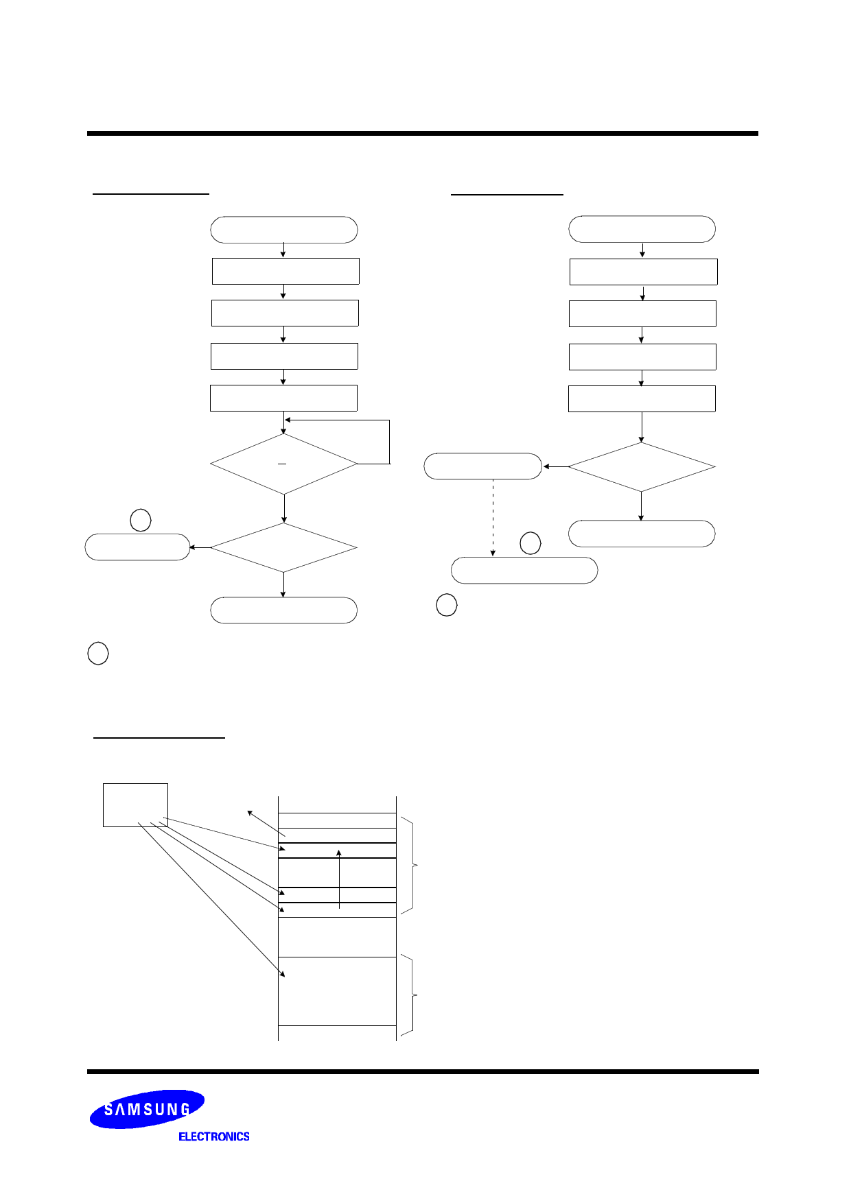
Erase Flow Chart
Start
Write 60H
Write Block Address
Write D0H
Write 70H
FLASH MEMORY
Read Flow Chart
Start
Write 00H
Write Address
Read Data
ECC Generation
SR. 6 = 1 ?
or R/B = 1 ?
No
* No
Erase Error
Yes
SR. 0 = 0 ?
Yes
Erase Completed
No
Reclaim the Error
Verify ECC
Yes
Page Read Completed
*
Block Replacement
* : copy the corrected whole block data to another
block (recommended for high reliability system)
* : If erase operation results in an error, map out
the failing block and replace it with another block.
Block Replacement
Buffer
memory
error occurs
Block A
When the error happens in Block "A", try to write the
data into another Block "B" by reloading from an exter-
nal buffer. Then, prevent further system access to
Block "A"(by creating a "invalid block" table or other
appropriate scheme.)
Block B
11
11 Page | ||
| Páginas | Total 26 Páginas | |
| PDF Descargar | [ Datasheet KM29U128T.PDF ] | |
Hoja de datos destacado
| Número de pieza | Descripción | Fabricantes |
| KM29U128IT | 16M x 8 Bit NAND Flash Memory | Samsung semiconductor |
| KM29U128T | 16M x 8 Bit NAND Flash Memory | Samsung semiconductor |
| Número de pieza | Descripción | Fabricantes |
| SLA6805M | High Voltage 3 phase Motor Driver IC. |
Sanken |
| SDC1742 | 12- and 14-Bit Hybrid Synchro / Resolver-to-Digital Converters. |
Analog Devices |
|
DataSheet.es es una pagina web que funciona como un repositorio de manuales o hoja de datos de muchos de los productos más populares, |
| DataSheet.es | 2020 | Privacy Policy | Contacto | Buscar |
