|
|
|
PDF IDT70V26 Data sheet ( Hoja de datos )
| Número de pieza | IDT70V26 | |
| Descripción | HIGH-SPEED 3.3V 16K x 16 DUAL-PORT STATIC RAM | |
| Fabricantes | Integrated Device Technology | |
| Logotipo | ||
Hay una vista previa y un enlace de descarga de IDT70V26 (archivo pdf) en la parte inferior de esta página. Total 17 Páginas | ||
|
No Preview Available !
HIGH-SPEED 3.3V
16K x 16 DUAL-PORT
STATIC RAM
IDT70V26S/L
Features
x True Dual-Ported memory cells which allow simultaneous
reads of the same memory location
x High-speed access
– Commercial: 25/35/55ns (max.)
x Low-power operation
– IDT70V26S
Active: 300mW (typ.)
Standby: 3.3mW (typ.)
– IDT70V26L
Active: 300mW (typ.)
Standby: 660µW (typ.)
x Separate upper-byte and lower-byte control for multiplexed
bus compatibility
x IDT70V26 easily expands data bus width to 32 bits or more
using the Master/Slave select when cascading more than
one device
x M/S = VIH for BUSY output flag on Master
M/S = VIL for BUSY input on Slave
x On-chip port arbitration logic
x Full on-chip hardware support of semaphore signaling
between ports
x Fully asynchronous operation from either port
x TTL-compatible, single 3.3V (±0.3V) power supply
x Available in 84-pin PGA and PLCC
x Industrial temperature range (-40°C to +85°C) is available
for selected speeds
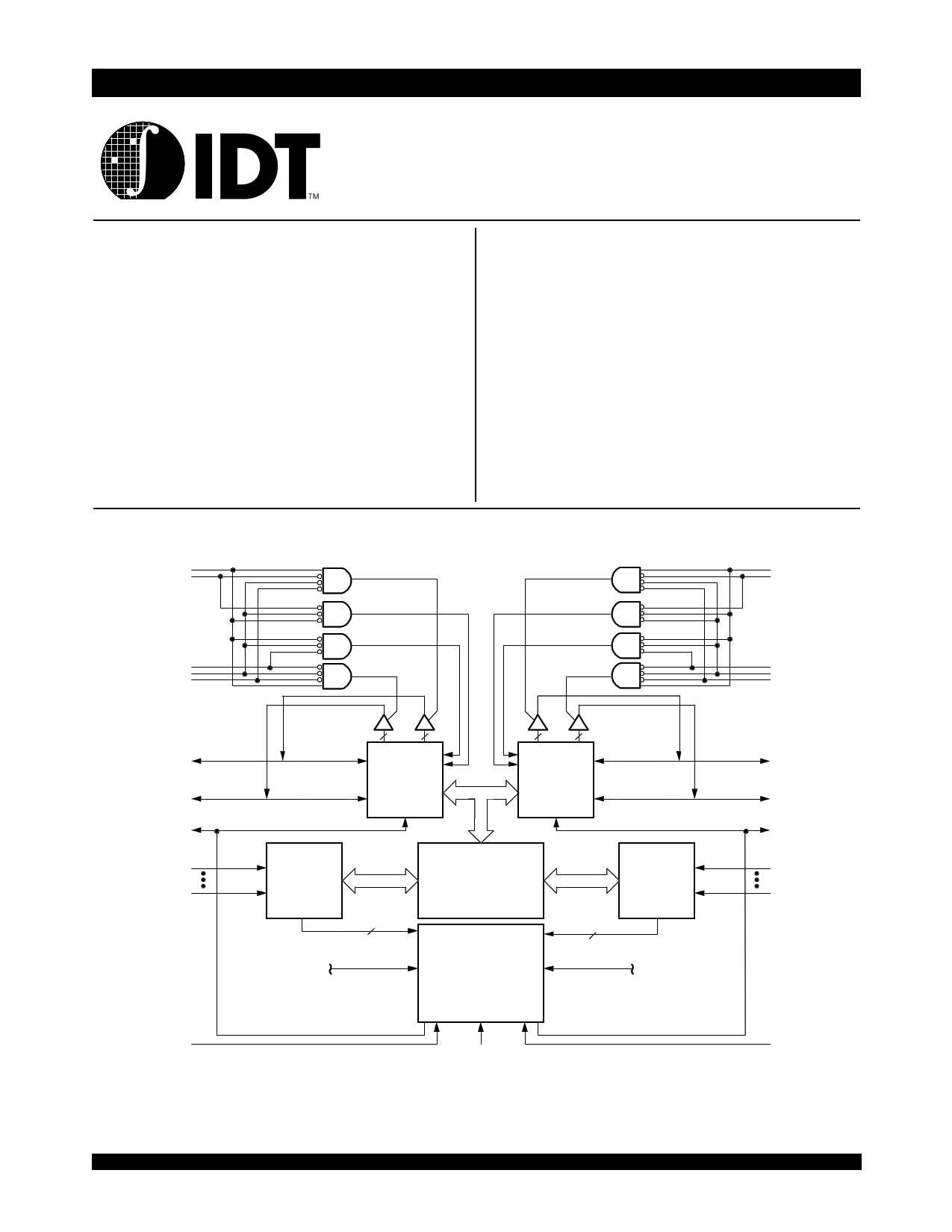
Functional Block Diagram
R/WL
UBL
R/WR
UBR
LBL
CEL
OEL
I/O8L-I/O15L
I/O0L-I/O7L
BUSYL(1,2)
A13L
A0L
I/O
Control
I/O
Control
Address
Decoder
14
CEL
MEMORY
ARRAY
ARBITRATION
SEMAPHORE
LOGIC
Address
Decoder
14
CER
SEML
NOTES:
1. (MASTER): BUSY is output; (SLAVE): BUSY is input.
2. BUSY outputs are non-tri-stated push-pull.
M/S
©2000 Integrated Device Technology, Inc.
1
LBR
CER
OER
I/O8R-I/O15R
I/O0R-I/O7R
BUSYR(1,2)
A13R
A0R
SEMR
2945 drw 01
JUNE 2000
DSC 2945/13
1 page 
IDT70V26S/L
High-Speed 16K x 16 Dual-Port Static RAM
Industrial and Commercial Temperature Ranges
Absolute Maximum Ratings(1)
Symbol
Rating
Commercial
& Industrial
VTERM(2)
Terminal Voltage
with Respect
to GND
-0.5 to +4.6
TBIAS
Temperature
Under Bias
-55 to +125
TSTG Storage
Temperature
-65 to +150
IOUT DC Output
Current
50
Unit
V
oC
oC
mA
Maximum Operating Temperature
and Supply Voltage(1,2)
Grade
GND
Ambient Temperature
Vcc
Commercial
0OC to +70OC
0V 3.3V + 0.3
Industrial
-40OC to +85OC
0V 3.3V + 0.3
NOTES:
2945 tbl 05
1. This is the parameter TA. This is the "instant on" case temperature.
2. Industrial temperature: for specific speeds, packages and powers contact your
sales office.
NOTES:
2945 tbl 04
1. Stresses greater than those listed under ABSOLUTE MAXIMUM RATINGS may
cause permanent damage to the device. This is a stress rating only and functional
operation of the device at these or any other conditions above those indicated in
the operational sections of this specification is not implied. Exposure to absolute
maximum rating conditions for extended periods may affect reliability.
2. VTERM must not exceed Vcc + 0.3V for more than 25% of the cycle time or 10ns
maximum, and is limited to < 20mA for the period of VTERM > Vcc + 0.3V.
Recommended DC Operating
Conditions(2)
Symbol
Parameter
Min. Typ.
Max.
VCC Supply Voltage
3.0 3.3
3.6
Unit
V
GND Ground
VIH Input High Voltage
00
0V
2.0 ____ VCC + 0.3(2) V
Capacitance(1) (TA = +25°C, f = 1.0MHz)
Symbol
Parameter
Conditions(2) Max. Unit
CIN Input Capacitance
VIN = 3dV
9 pF
VIL Input Low Voltage
-0.3(1)
NOTES:
1. VIL > -1.5V for pulse width less than 10ns.
2. VTERM must not exceed Vcc + 0.3V.
____
0.8 V
2945 tbl 06
COUT Output Capacitance
VOUT = 3dV
10 pF
NOTES:
2945 tbl 07
1. This parameter is determined by device characterization but is not production
tested.
2. 3dV represents the interpolated capacitance when the input and output signals
switch from 0V to 3V or from 3V to 0V.
DC Electrical Characteristics Over the Operating
Temperature and Supply Voltage Range (VCC = 3.3V ± 0.3V)
70V26S
Symbol
Parameter
Test Conditions
Min. Max.
|ILI| Input Leakage Current(1)
VCC = 3.6V, VIN = 0V to VCC
___ 10
|ILO| Output Leakage Current
CE = VIH, VOUT = 0V to VCC
___ 10
VOL Output Low Voltage
IOL = +4mA
___ 0.4
VOH Output High Voltage
IOH = -4mA
2.4 ___
NOTE:
1. At VCC < 2.0V, input leakages are undefined.
70V26L
Min. Max.
___ 5
___ 5
___ 0.4
2.4 ___
Unit
µA
µA
V
V
2945 tbl 08
6.542
5 Page 
IDT70V26S/L
High-Speed 16K x 16 Dual-Port Static RAM
Industrial and Commercial Temperature Ranges
AC Electrical Characteristics Over the
Operating Temperature and Supply Voltage Range(6,7)
70V26X25
Com'l Only
70V26X35
Com'l Only
70V26X55
Com'l Only
Symbol
BUSY TIMING (M/S = VIH)
Parameter
Min. Max. Min. Max. Min. Max. Unit
tBAA BUSY Access Time from Address Match
____ 25 ____ 35 ____ 45 ns
tBDA BUSY Disable Time from Address Not Match
____ 25 ____ 35 ____ 45 ns
tBAC BUSY Acce ss Time from Chip Enable Low
____ 25 ____ 35 ____ 45 ns
tBDC BUSY Disab le Time from Chip Enable High
____ 25 ____ 35 ____ 45 ns
tAPS Arbitration Priority Set-up Time(2)
5 ____ 5 ____ 5 ____ ns
tBDD BUSY Disable to Valid Data(3)
tWH Write Hold After BUSY(5)
BUSY INPUT TIMING (M/S = VIL)
____ 35 ____ 40 ____ 50 ns
20 ____ 25 ____ 25 ____ ns
tWB BUSY Input to Write(4)
tWH Write Hold After BUSY(5)
0 ____ 0 ____ 0 ____ ns
20 ____ 25 ____ 25 ____ ns
PORT-TO-PORT DELAY TIMING
tWDD Write Pulse to Data Delay(1)
tDDD Write Data Valid to Read Data Delay(1)
____ 55 ____ 65 ____ 85 ns
____ 50 ____ 60 ____ 80 ns
NOTES:
1. Port-to-port delay through RAM cells from writing port to reading port, refer to "Timing Waveform of Write with Port-to-Port Read and BUSY (M/S = VIH)".
2. To ensure that the earlier of the two ports wins.
3. tBDD is a calculated parameter and is the greater of 0, tWDD – tWP (actual) or tDDD – tDW (actual).
4. To ensure that the write cycle is inhibited on port "B" during contention on port "A".
5. To ensure that a write cycle is completed on port "B" after contention on port "A".
6. 'X' in part number indicates power rating (S or L).
7. Industrial temperature: for specific speeds, packages and powers contact your sales office.
2945 tbl 13
Timing Waveform of Write with Port-to-Port Read and BUSY(2,4,5)
tWC
ADDR"A"
MATCH
tWP
R/W"A"
tDW tDH
DATAIN "A"
tAPS (1)
VALID
ADDR"B"
BUSY"B"
tBAA
MATCH
tBDA
tWDD
DATAOUT "B"
NOTES:
tDDD(3)
1. To ensure that the earlier of the two ports wins. tAPS is ignored for M/S = VIL (SLAVE).
2. CEL = CER = VIL
3. OE = VIL for the reading port.
4. If M/S = VIL (SLAVE), then BUSY is an input (BUSY"A" = VIH and BUSY"B" = "don't care", for this example).
5. All timing is the same for left and right ports. Port "A" may be either the left or right port. Port "B" is the port opposite from port "A".
tBDD
VALID
2945 drw 12
61.412
11 Page | ||
| Páginas | Total 17 Páginas | |
| PDF Descargar | [ Datasheet IDT70V26.PDF ] | |
Hoja de datos destacado
| Número de pieza | Descripción | Fabricantes |
| IDT70V24 | HIGH-SPEED 3.3V 4K x 16 DUAL-PORT STATIC RAM | Integrated Device Technology |
| IDT70V25 | HIGH-SPEED 3.3V 8K x 16 DUAL-PORT STATIC RAM | Integrated Device Technology |
| IDT70V26 | HIGH-SPEED 3.3V 16K x 16 DUAL-PORT STATIC RAM | Integrated Device Technology |
| IDT70V261L | HIGH-SPEED 3.3V 16K x 16 DUAL-PORT STATIC RAM | Integrated Device Technology |
| Número de pieza | Descripción | Fabricantes |
| SLA6805M | High Voltage 3 phase Motor Driver IC. |
Sanken |
| SDC1742 | 12- and 14-Bit Hybrid Synchro / Resolver-to-Digital Converters. |
Analog Devices |
|
DataSheet.es es una pagina web que funciona como un repositorio de manuales o hoja de datos de muchos de los productos más populares, |
| DataSheet.es | 2020 | Privacy Policy | Contacto | Buscar |