|
|
|
PDF IDT723611 Data sheet ( Hoja de datos )
| Número de pieza | IDT723611 | |
| Descripción | CMOS SyncFIFO 64 x 36 | |
| Fabricantes | Integrated Device Technology | |
| Logotipo | ||
Hay una vista previa y un enlace de descarga de IDT723611 (archivo pdf) en la parte inferior de esta página. Total 20 Páginas | ||
|
No Preview Available !
CMOS SyncFIFO
64 x 36
IDT723611
Integrated Device Technology, Inc.
FEATURES:
• Free-running CLKA and CLKB may be asynchronous or
coincident (permits simultaneous reading and writing of
data on a single clock edge)
• 64 x 36 storage capacity
• Synchronous data buffering from Port A to Port B
• Mailbox bypass register in each direction
• Programmable Almost-Full (AF) and Almost-Empty (AE)
flags
• Microprocessor Interface Control Logic
• Full Flag (FF) and Almost-Full (AF) flags synchronized by
CLKA
• Empty Flag (EF) and Almost-Empty (AE) flags synchro-
nized by CLKB
• Passive parity checking on each Port
• Parity Generation can be selected for each Port
• Supports clock frequencies up to 67MHz
• Fast access times of 10ns
• Available in 132-pin Plastic Quad Flatpack (PQF) or
space-saving 120-pin Thin Quad Flatpack (PF)
• Low-power advanced CMOS technology
• Industrial temperature range (-40oC to +85oC) is avail-
able, tested to military elecrical specifications
DESCRIPTION:
The IDT723611 is a monolithic, high-speed, low-power,
CMOS Synchronous (clocked) FIFO memory which supports
clock frequencies up to 67MHz and has read access times as
fast as 10ns. The 64 x 36 dual-port FIFO buffers data from Port
A to Port B. The FIFO has flags to indicate empty and full
conditions, and two programmable flags, Almost-Full (AF) and
Almost-Empty (AE), to indicate when a selected number of
words is stored in memory. Communication between each
port can take place through two 36-bit mailbox registers. Each
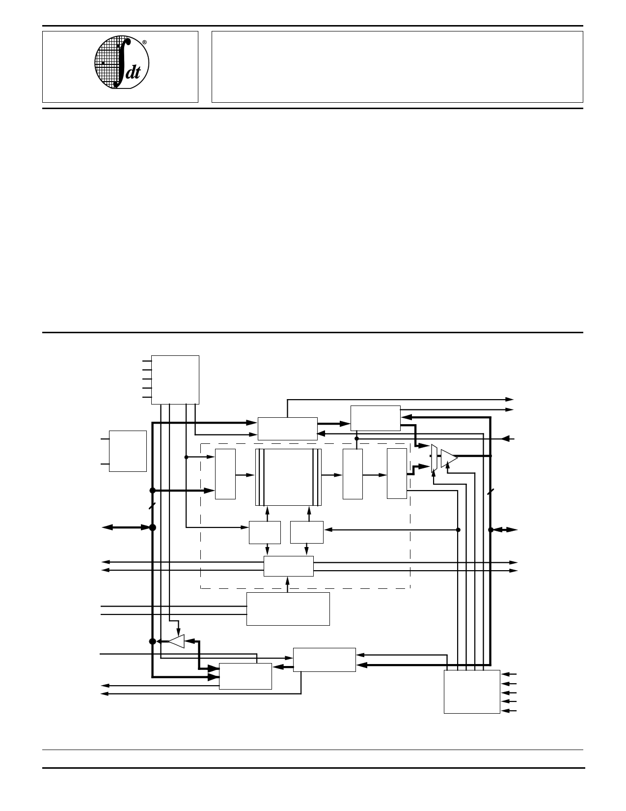
FUNCTIONAL BLOCK DIAGRAM
CLKA
CSA
W/RA
ENA
MBA
Port-A
Control
Logic
RST
ODD/
EVEN
Reset
Logic
A0 - A35
36
Mail 1
Register
64 x 36
SRAM
Write Read
Pointer Pointer
Parity
Gen/Check
MBF1
PEFB
PGB
•
36
B0 - B35
FF Status Flag
AF Logic
FIFO
FS0
FS1
Programmable
Flag Offset
Registers
EF
AE
PGA
PEFA
MBF2
Parity
Gen/Check
Mail 2
Register
Port-B
Control
Logic
SyncFIFO is a trademark and the IDT logo is a registered trademark of Integrated Device Technology, Inc.
COMMERCIAL TEMPERATURE RANGE
©1997 Integrated Device Technology, Inc.
For latest information contact IDT's web site at www.idt.com or fax-on-demand at 408-492-8391.
CLKB
CSB
W/RB
ENB
MBB
3024 drw 01
MAY 1997
DSC-3024/4
1
1 page 
IDT723611 CMOS SyncFIFO™
64 x 36
PIN DESCRIPTION (CONTINUED)
COMMERCIAL TEMPERATURE RANGES
Symbol
MBF2
ODD/
EVEN
PEFA
PEFB
PGA
PGB
RST
W/RA
W/RB
Name
Mail2 Register Flag
Odd/Even Parity
Select
Port-A Parity Error
Flag
Port-B Parity Error
Flag
Port-A Parity
Generation
Port-B Parity
Generation
Reset
Port-A Write/Read
Select
Port-B Write/Read
Select
I/O Description
O MBF2 is set LOW by a LOW-to-HIGH transition of CLKB that writes data to
the mail2 register. Writes to the mail2 register are inhibited while MBF2 is
LOW. MBF2 is set HIGH by a LOW-to-HIGH transition of CLKA when a port-
A read is selected and MBA is HIGH. MBF2 is set HIGH when the device is
reset.
I Odd parity is checked on each port when ODD/EVEN is HIGH, and even
parity is checked when ODD/EVEN is LOW. ODD/EVEN also selects the
type of parity generated for each port if parity generation is enabled for a read
operation.
O When any byte applied to terminals A0-A35 fails parity, PEFA is LOW.
(Port A) Bytes are organized as A0-A8, A9-A17, A18-A26, and A27-A35, with the
most significant bit of each byte serving as the parity bit. The type of parity
checked is determined by the state of the ODD/EVEN input. The parity trees
used to check the A0-A35 inputs are shared by the mail2 register to generate
parity if parity generation is selected by PGA. Therefore, if a mail2 read with
parity generation is setup by having CSA LOW, ENA HIGH, W/RA LOW, MBA
HIGH, and PGA HIGH, the PEFA flag is forced HIGH regardless of the state of
A0-A35 inputs.
O When any byte applied to terminals B0-B35 fails parity, PEFB is LOW.
(Port B) Bytes are organized as B0-B8, B9-B17, B18-B26, B27-B35, with the most
significant bit of each byte serving as the parity bit. The type of parity
checked is determined by the state of the ODD/EVEN input. The parity trees
used to check the B0-B35 inputs are shared by the mail1 register to generate
parity if parity generation is selected by PGB. Therefore, if a mail1 read with
parity generation is setup by having CSB LOW, ENB HIGH, W/RB LOW,
MBB HIGH, and PGB HIGH, the PEFB flag is forced HIGH regardless of the
state of the B0-B35 inputs
I Parity is generated for mail2 register reads from port A when PGA is HIGH.
The type of parity generated is selected by the state of the ODD/EVEN input.
Bytes are organized as A0-A8, A9-A17, A18-A26, and A27-A35. The gener-
ated parity bits are output in the most significant bit of each byte.
I Parity is generated for data reads from port B when PGB is HIGH. The type
of parity generated is selected by the state of the ODD/EVEN input. Bytes are
organized as B0-B8, B9-B17, B18-B26, and B27-B35. The generated parity
bits are output in the most significant bit of each byte.
I To reset the device, four LOW-to-HIGH transitions of CLKA and four LOW-to-
HIGH transitions of CLKB must occur while RST is LOW. This sets the AF,
MBF1, and MBF2 flags HIGH and the EF, AE, and FF flags LOW. The LOW-
to-HIGH transition of RST latches the status of the FS1 and FS0 inputs to
select almost-full and almost-empty flag offset.
I A HIGH selects a write operation and a LOW selects a read operation on
port A for a LOW-to-HIGH transition of CLKA. The A0-A35 outputs are in the
high-impedance state when W/RA is HIGH.
I A HIGH selects a write operation and a LOW selects a read operation on
port B for a LOW-to-HIGH transition of CLKB. The B0-B35 outputs are in the
high-impedance state when W/RB is HIGH.
5
5 Page 
IDT723611 CMOS SyncFIFO™
64 x 36
COMMERCIAL TEMPERATURE RANGES
empty offset register (X). This register is loaded with one of
four preset values during a device reset (see reset above).
The almost-full flag is LOW when the FIFO contains (64-X) or
more words in memory and is HIGH when the FIFO contains
[64-(X+1)] or less words.
Two LOW-to-HIGH transitions on the port-A clock (CLKA)
are required after a FIFO read for the almost-full flag to reflect
the new level of fill. Therefore, the almost-full flag of a FIFO
containing [64-(X+1)] or less words remains LOW if two CLKA
cycles have not elapsed since the read that reduced the
number of words in memory to [64-(X+1)]. The almost-full flag
is set HIGH by the second CLKA LOW-to-HIGH transition
after the FIFO read that reduces the number of words in
memory to [64-(X+1)]. A LOW-to-HIGH transition on CLKA
begins the first synchronization cycle if it occurs at time tSKEW2
or greater after the read that reduces the number of words in
memory to [64-(X+1)]. Otherwise, the subsequent CLKA
cycle can be the first synchronization cycle (see figure 7).
MAILBOX REGISTERS
Two 36-bit bypass registers are on the IDT723611 to pass
command and control information between port A and port B.
The mailbox-select (MBA, MBB) inputs choose between a
mail register and a FIFO for a port data transfer operation. A
LOW-to-HIGH transition on CLKA writes A0-A35 data to the
mail1 register when port-A write is selected by CSA, W/RA,
and ENA with MBA HIGH. A LOW-to-HIGH transition on
CLKB writes B0-B35 data to the mail2 register when port-B
write is selected by CSB, W/RB, and ENB with MBB HIGH.
Writing data to a mail register sets its corresponding flag
(MBF1 or MBF2) LOW. Attempted writes to a mail register are
ignored while its mail flag is LOW.
When the port-B data (B0-B35) outputs are active, the data
on the bus comes from the FIFO output register when the port-
B mailbox select (MBB) input is LOW and from the mail1
register when MBB is HIGH. Mail2 data is always present on
the port-A data (A0-A35) outputs when they are active. The
mail1 register flag (MBF1) is set HIGH by a LOW-to-HIGH
transition on CLKB when a port-B read is selected by CSB, W/
RB, and ENB with MBB HIGH. The mail2 register flag (MBF2)
is set HIGH by a LOW-to-HIGH transition on CLKA when a
port-A read is selected by CSA, W/RA, and ENA with MBA
HIGH. The data in a mail register remains intact after it is read
and changes only when new data is written to the register.
PARITY CHECKING
The port-A (A0-A35) inputs and port-B (B0-B35) inputs
each have four parity trees to check the parity of incoming (or
outgoing) data. A parity failure on one or more bytes of the
input bus is reported by a LOW level on the port parity error flag
(PEFA, PEFB). Odd or even parity checking can be selected,
and the parity error flags can be ignored if this feature is not
desired.
Parity status is checked on each input bus according to the
level of the odd/even parity (ODD/EVEN) select input. A parity
error on one or more bytes of a port is reported by a LOW level
on the corresponding port parity error flag (PEFA, PEFB)
output. Port-A bytes are arranged as A0-A8, A9-A17, A18-
A26, and A27-A35, and port-B bytes are arranged as B0-B8,
B9-B17, B18-B26, and B27-B35. When odd/even parity is
selected, a port parity error flag (PEFA, PEFB) is LOW if any
byte on the port has an odd/even number of LOW levels
applied to its bits.
The four parity trees used to check the A0-A35 inputs are
shared by the mail2 register when parity generation is se-
lected for port-A reads (PGA=HIGH). When port-A read from
the mail2 register with parity generation is selected with CSA
LOW, ENA HIGH, W/RA LOW, MBA HIGH, and PGA HIGH,
the port-A parity error flag (PEFA) is held HIGH regardless of
the levels applied to the A0-A35 inputs. Likewise, the parity
trees used to check the B0-B35 inputs are shared by the mail1
register when parity generation is selected for port-B reads
(PGB=HIGH). When a port-B read from the mail1 register with
parity generation is selected with CSB LOW, ENB HIGH, W/
RB LOW, MBB HIGH, and PGB HIGH, the port-B parity error
flag (PEFB) is held HIGH regardless of the levels applied to the
B0-B35 inputs.
PARITY GENERATION
A HIGH level on the port-A parity generate select (PGA) or
port-B generate select (PGB) enables the IDT723611 to
generate parity bits for port reads from a FIFO or mailbox
register. Port-A bytes are arranged as A0-A8, A9-A17, A18-
A26, and A27-A35, with the most significant bit of each byte
used as the parity bit. Port-B bytes are arranged as B0-B8, B9-
B17, B18-B26, and B27-B35, with the most significant bit of
each byte used as the parity bit. A write to a FIFO or mail
register stores the levels applied to all thirty-six inputs regard-
less of the state of the parity generate select (PGA, PGB)
inputs. When data is read from a port with parity generation
selected, the lower eight bits of each byte are used to generate
a parity bit according to the level on the ODD/EVEN select.
The generated parity bits are substituted for the levels origi-
nally written to the most significant bits of each byte as the
word is read to the data outputs.
Parity bits for FIFO data are generated after the data is
read from SRAM and before the data is written to the output
register. Therefore, the port-B parity generate select (PGB)
and ODD/EVEN have setup and hold time constraints to the
port-B clock (CLKB) for a rising edge of CLKB used to read a
new word to the FIFO output register.
The circuit used to generate parity for the mail1 data is
shared by the port-B bus (B0-B35) to check parity and the
circuit used to generate parity for the mail2 data is shared by
the port-A bus (A0-A35) to check parity. The shared parity
trees of a port are used to generate parity bits for the data in
a mail register when the port write/read select (W/RA, W/RB)
input is LOW, the port mail select (MBA, MBB) input is HIGH,
chip select (CSA, CSB) is LOW, enable (ENA, ENB) is HIGH,
and the port parity generate select (PGA, PGB) is HIGH.
Generating parity for mail register data does not change the
contents of the register.
11
11 Page | ||
| Páginas | Total 20 Páginas | |
| PDF Descargar | [ Datasheet IDT723611.PDF ] | |
Hoja de datos destacado
| Número de pieza | Descripción | Fabricantes |
| IDT723611 | CMOS SyncFIFO 64 x 36 | Integrated Device Technology |
| IDT723612 | BiCMOS SyncBiFIFOO 64 x 36 x 2 | Integrated Device Technology |
| IDT723612L15PF | BiCMOS SyncBiFIFOO 64 x 36 x 2 | Integrated Device Technology |
| IDT723612L15PQF | BiCMOS SyncBiFIFOO 64 x 36 x 2 | Integrated Device Technology |
| Número de pieza | Descripción | Fabricantes |
| SLA6805M | High Voltage 3 phase Motor Driver IC. |
Sanken |
| SDC1742 | 12- and 14-Bit Hybrid Synchro / Resolver-to-Digital Converters. |
Analog Devices |
|
DataSheet.es es una pagina web que funciona como un repositorio de manuales o hoja de datos de muchos de los productos más populares, |
| DataSheet.es | 2020 | Privacy Policy | Contacto | Buscar |