|
|
|
PDF IDT72271 Data sheet ( Hoja de datos )
| Número de pieza | IDT72271 | |
| Descripción | CMOS SUPERSYNC FIFOO 16/384 x 9/ 32/768 x 9 | |
| Fabricantes | Integrated Device Technology | |
| Logotipo | ||
Hay una vista previa y un enlace de descarga de IDT72271 (archivo pdf) en la parte inferior de esta página. Total 30 Páginas | ||
|
No Preview Available !
CMOS SUPERSYNC FIFO™
16,384 x 9, 32,768 x 9
IDT72261
IDT72271
Integrated Device Technology, Inc.
FEATURES:
• 16,384 x 9-bit storage capacity (IDT72261)
• 32,768 x 9-bit storage capacity (IDT72271)
• 10ns read/write cycle time (8ns access time)
• Retransmit Capability
• Auto power down reduces power consumption
• Master Reset clears entire FIFO, Partial Reset clears
data, but retains programmable settings
• Empty, Full and Half-full flags signal FIFO status
• Programmable Almost Empty and Almost Full flags, each
flag can default to one of two preselected offsets
• Program partial flags by either serial or parallel means
• Select IDT Standard timing (using EF and FF flags) or
First Word Fall Through timing (using OR and IR flags)
• Easily expandable in depth and width
• Independent read and write clocks (permit simultaneous
reading and writing with one clock signal
• Available in the 64-pin Thin Quad Flat Pack (TQFP), 64-
pin Slim Thin Quad Flat Pack (STQFP) and the 68-pin
Pin Grid Array (PGA)
• Output enable puts data outputs into high impedance
• High-performance submicron CMOS technology
• Industrial temperature range (-40OC to +85OC) is avail-
able, tested to military electrical specifications
DESCRIPTION:
The IDT72261/72271 are monolithic, CMOS, high capac-
ity, high speed, low power first-in, first-out (FIFO) memories
with clocked read and write controls. These FIFOs are
applicable for a wide variety of data buffering needs, such as
optical disk controllers, local area networks (LANs), and inter-
processor communication.
Both FIFOs have a 9-bit input port (Dn) and a 9-bit output
port (Qn). The input port is controlled by a free-running clock
(WCLK) and a data input enable pin (WEN). Data is written
into the synchronous FIFO on every clock when WEN is
asserted. The output port is controlled by another clock pin
(RCLK) and enable pin (REN). The read clock can be tied to
the write clock for single clock operation or the two clocks can
run asynchronously for dual clock operation. An output
enable pin (OE) is provided on the read port for three-state
control of the outputs.
The IDT72261/72271 have two modes of operation: In the
IDT Standard Mode, the first word written to the FIFO is
deposited into the memory array. A read operation is required
to access that word. In the First Word Fall Through Mode
(FWFT), the first word written to an empty FIFO appears
automatically on the outputs, no read operation required. The
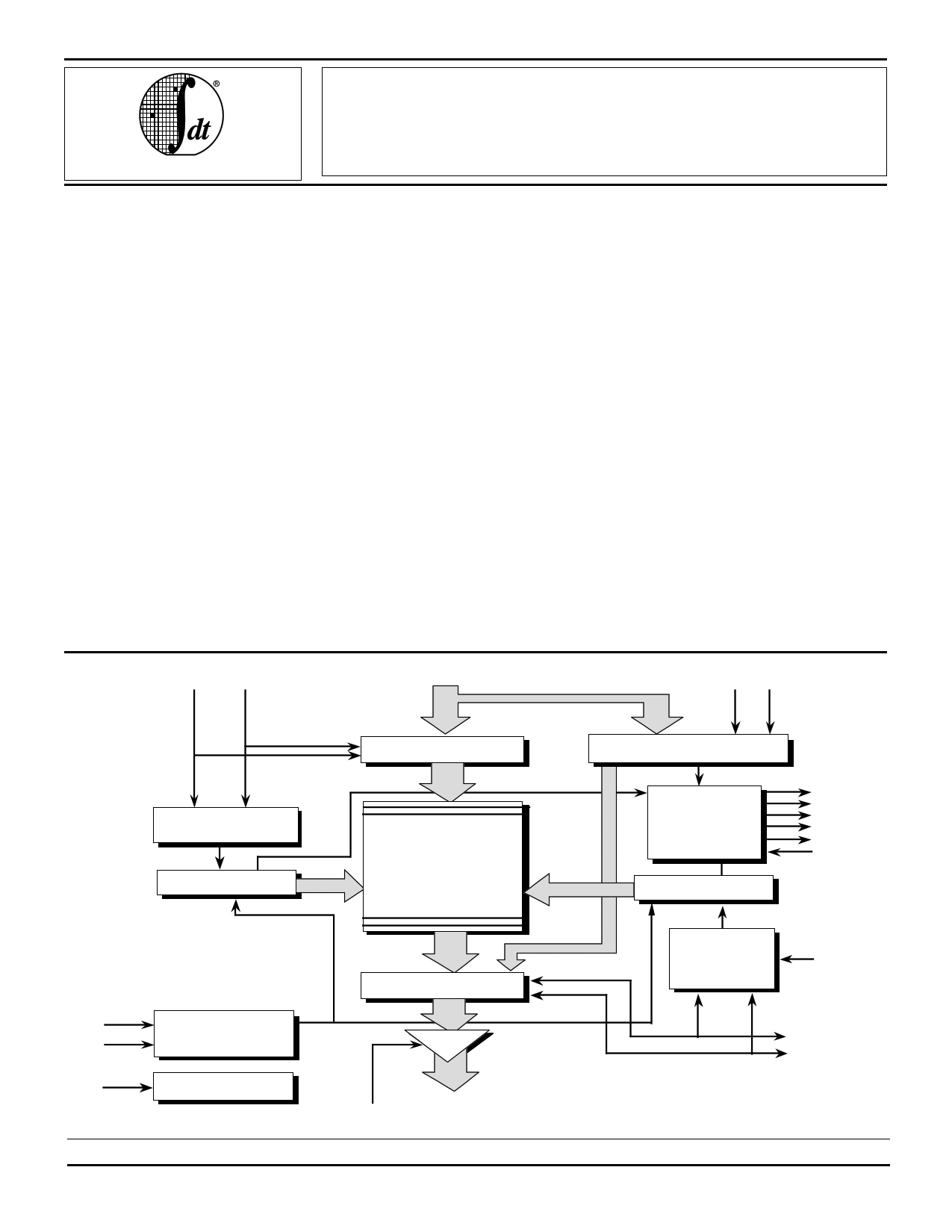
FUNCTIONALWBENLOCWKCDLKIAGRAM
D0-D8
LD SEN
•
•
INPUT REGISTER
OFFSET REGISTER
WRITE CONTROL
LOGIC
WRITE POINTER
••
RAM ARRAY
16,384 x 9
32,768 x 9
••
OUTPUT REGISTER
FLAG
LOGIC
READ POINTER
READ
CONTROL
LOGIC
MRS
PRS
RESET LOGIC
•
•
FS TIMING
OE Q0-Q8
SuperSyncFIFO is a trademark and the IDT logo is a registered trademark of Integrated Device Technology, Inc.
MILITARY AND COMMERCIAL TEMPERATURE RANGES
©1997 Integrated Device Technology, Inc
For latest information contact IDT's web site at www.idt.com or fax-on-demand at 408-492-8391.
•
FF/IR
PAF
EPAF/EOR
HF
FWFT/SI
RT
RCLK
REN
3036 drw 01
MAY 1997
DSC-3036/6
1
1 page 
IDT72261/72271 SyncFIFO™
16,384 x 9, 32,768 x 9
MILITARY AND COMMERCIAL TEMPERATURE RANGES
ABSOLUTE MAXIMUM RATINGS(1)
Symbol
Rating
Commercial MIilitary Unit
VTERM Terminal Voltage –0.5 to +7.0 –0.5 to +7.0 V
with respect to GND
TA Operating
Temperature
0 to +70 –55 to +125 °C
TBIAS
Temperature Under –55 to +125 –65 to +135 °C
Bias
TSTG
Storage
Temperature
–55 to +125 –65 to +155 °C
IOUT DC Output Current
50
50 mA
NOTE:
3097 tbl 02
1. Stresses greater than those listed under ABSOLUTE MAXIMUM RAT-
INGS may cause permanent damage to the device. This is a stress rating only
and functional operation of the device at these or any other conditions above
those indicated in the operational sections of this specification is not implied.
Exposure to absolute maimum rating conditions for extended periods may
affect reliabilty.
RECOMMENDED DC
OPERATING CONDITIONS
Symbol
VCCM
VCCC
Parameter
Military Supply
Voltage
Commercial Supply
Voltage
Min. Typ. Max. Unit
4.5 5.0 5.5 V
4.5 5.0 5.5 V
GND Supply Voltage
0 0 0V
VIH Input High Voltage
2.0 — — V
Commercial
VIH Input High Voltage
2.2 — — V
Military
VIL(1) Input Low Voltage
— — 0.8 V
Commercial & Military
NOTE:
3097 tbl 03
1. 1.5V undershoots are allowed for 10ns once per cycle.
DC ELECTRICAL CHARACTERISTICS
(Commercial: VCC = 5V ± 10%, TA = 0°C to +70°C; Military: VCC = 5V ± 10%, TA = –55°C to +125°C)
Symbol
Parameter
ILI(1) Input Leakage Current (any input)
ILO(2) Output Leakage Current
VOH Output Logic “1” Voltage, IOH = –2 mA
VOL Output Logic “0” Voltage, IOL = 8 mA
ICC1(3) Active Power Supply Current
ICC2(3,4) Power Down Current (All inputs = VCC - 0.2V or
GND + 0.2V, RCLK and WCLK are free-running)
NOTES:
1. Measurements with 0.4 ≤ VIN ≤ VCC.
2. OE = VIH
3. Tested at f = 20 MHz with outputs unloaded.
4. No data written or read for more than 10 cycles
DT72261L
IDT72271L
Commercial
tCLK = 10, 12,15, 20ns
Min. Typ. Max.
–1 —
1
–10 —
10
2.4 — —
— — 0.4
— — 150
— — 15
IDT72261L
IDT72271L
Military
tCLK = 15, 25ns
Min. Typ. Max.
–10 —
10
–10 —
10
2.4 —
—
— — 0.4
— — 200
— — 25
Unit
µA
µA
V
V
mA
mA
3097 tbl 04
CAPACITANCE (TA = +25°C, f = 1.0MHz)
Symbol Parameter(1) Conditions
Max.
CIN(2)
COUT(1,2)
Input
Capacitance
Output
Capacitance
VIN = 0V
VOUT = 0V
10
10
NOTES:
1. With output deselected, (OE=HIGH).
2. Characterized values, not currently tested.
Unit
pF
pF
3097 tbl 05
5
5 Page 
IDT72261/72271 SyncFIFO™
16,384 x 9, 32,768 x 9
MILITARY AND COMMERCIAL TEMPERATURE RANGES
equal to or less than the cycle period of the non-selected
clock.
The selected clock must be continuous. It is, however,
permissible to stop the non-selected clock. Note, so long as
RCLK is idle, EF/OR and PAE will not be updated. Likewise,
as long as WCLK is idle, FF/IR and PAF will not be updated.
Changing the FS setting during FIFO operation (i.e. read-
ing or writing) is not permitted; however, such a change at the
time of Master Reset or Partial Reset is all right. FS is an
asynchronous input.
OUTPUTS:
FULL FLAG (FF/IR)
This is a dual purpose pin. In IDT Standard Mode, the Full
Flag (FF) function is selected. When the FIFO is full (i.e. the
write pointer catches up to the read pointer), FF will go LOW,
inhibiting further write operation. When FF is HIGH, the FIFO
is not full. If no reads are performed after a reset (either MRS
or PRS), FF will go LOW after 16,384 writes tor the IDT72261
and 32,768 writes to the IDT72271.
In FWFT Mode, the Input Ready (IR) function is selected. IR
goes LOW when memory space is available for writing in
data. When there is no longer any free space left, IR goes
HIGH, inhibiting further write operation. If no reads are
performed after a reset (either MRS or PRS), IR will go HIGH
after 16,385 writes for the IDT72261 and 32,769 writes for the
IDT72271.
72261 – 16,384 x 9–BIT
87
0
EMPTY OFFSET (LSB) REG.
DEFAULT VALUE
07FH if LD is LOW at Master Reset
3FFH if LD is HIGH at Master Reset
The IR status not only measures the contents of the FIFO
memory, but also counts the presence of a word in the output
register. Thus, in FWFT mode, the total number of writes
necessary to deassert IR is one greater than needed to assert
FF in IDT Standard mode.
FF/IR is synchronized to WCLK. It is double-registered to
enhance metastable immunity.
EMPTY FLAG (EF/OR)
This is a dual purpose pin. In the IDT Standard Mode, the
Empty Flag (EF) function is selected. When the FIFO is empty
(i.e. the read pointer catches up to the write pointer), EF will go
LOW, inhibiting further read operations. When EF is HIGH,
the FIFO is not empty.
When writing the first word to an empty FIFO, the deassertion
time of EF is variable, and can be represent by the First Word
Latency parameter, tFWL1, which is measured from the rising
WCLK edge that writes the first word to the rising RCLK edge
that updates the flag. tFWL1 includes any delays due to clock
skew and can be expressed as follows:
tFWL1 max. = 10*Tf + 2*TRCLK (in ns)
where Tf is either the RCLK or the WCLK period, whichever
is shorter, and TRCLK is the RCLK period. Since no read can
take place until EF goes HIGH, the tFWL1 delay determines
how early the first word can be available at Qn. This delay has
no effect on the reading of subsequent words.
72271 – 32,768 x 9–BIT
87
0
EMPTY OFFSET (LSB) REG.
DEFAULT VALUE
07FH if LD is LOW at Master Reset
3FFH if LD is HIGH at Master Reset
85
08
6
0
EMPTY OFFSET (MSB) REG.
EMPTY OFFSET (MSB) REG.
00H 00H
87
08
7
0
FULL OFFSET (LSB) REG.
FULL OFFSET (LSB) REG.
DEFAULT VALUE
07FH if LD is LOW at Master Reset
3FFH if LD is HIGH at Master Reset
DEFAULT VALUE
07FH if LD is LOW at Master Reset
3FFH if LD is HIGH at Master Reset
85
8
0
6
0
FULL OFFSET (MSB) REG.
FULL OFFSET (MSB) REG.
00H
00H
3036 drw 06
3036 drw 05
NOTE:
1. Any bits of the offset register not being programmed should be set to zero.
Figure 3. Offset Register Location and Default Values
11
11 Page | ||
| Páginas | Total 30 Páginas | |
| PDF Descargar | [ Datasheet IDT72271.PDF ] | |
Hoja de datos destacado
| Número de pieza | Descripción | Fabricantes |
| IDT72271 | CMOS SUPERSYNC FIFOO 16/384 x 9/ 32/768 x 9 | Integrated Device Technology |
| IDT72274 | VARIABLE WIDTH SUPERSYNCO FIFO 8/192 x 18 or 16/384 x 9 16/384 x 18 or 32/768 x 9 | Integrated Device Technology |
| IDT72275 | (IDT72275 / IDT72285) CMOS SUPERSYNC FIFO | IDT |
| Número de pieza | Descripción | Fabricantes |
| SLA6805M | High Voltage 3 phase Motor Driver IC. |
Sanken |
| SDC1742 | 12- and 14-Bit Hybrid Synchro / Resolver-to-Digital Converters. |
Analog Devices |
|
DataSheet.es es una pagina web que funciona como un repositorio de manuales o hoja de datos de muchos de los productos más populares, |
| DataSheet.es | 2020 | Privacy Policy | Contacto | Buscar |