|
|
|
PDF IDT7217L Data sheet ( Hoja de datos )
| Número de pieza | IDT7217L | |
| Descripción | 16 x 16 PARALLEL CMOS MULTIPLIERS | |
| Fabricantes | Integrated Device Technology | |
| Logotipo | ||
Hay una vista previa y un enlace de descarga de IDT7217L (archivo pdf) en la parte inferior de esta página. Total 13 Páginas | ||
|
No Preview Available !
Integrated Device Technology, Inc.
16 x 16 PARALLEL
CMOS MULTIPLIERS
IDT7216L
IDT7217L
FEATURES:
• 16 x 16 parallel multiplier with double precision product
• 16ns clocked multiply time
• Low power consumption: 120mA
• Produced with advanced submicron CMOS high perfor-
mance technology
• IDT7216L is pin- and function compatible with TRW
MPY016H/K and AMD Am29516
• IDT7217L requires a single clock with register enables
making it pin- and function compatible with AMD
Am29517
• Configured for easy array expansion
• User-controlled option for transparent output register
mode
• Round control for rounding the MSP
• Input and output directly TTL-compatible
• Three-state output
• Available in Top Braze, DIP, PLCC, Flatpack and Pin
Grid Array
• Military product compliant to MIL-STD-883, Class B
• Standard Military Drawing #5962-86873 is listed on this
function for IDT7216 and Standard Military Drawing
#5962-87686 is listed for this function for IDT7217.
• Speeds available: Commercial: L16/20/25/35/45/55/65
Military:
L20/25/30/40/55/65/75
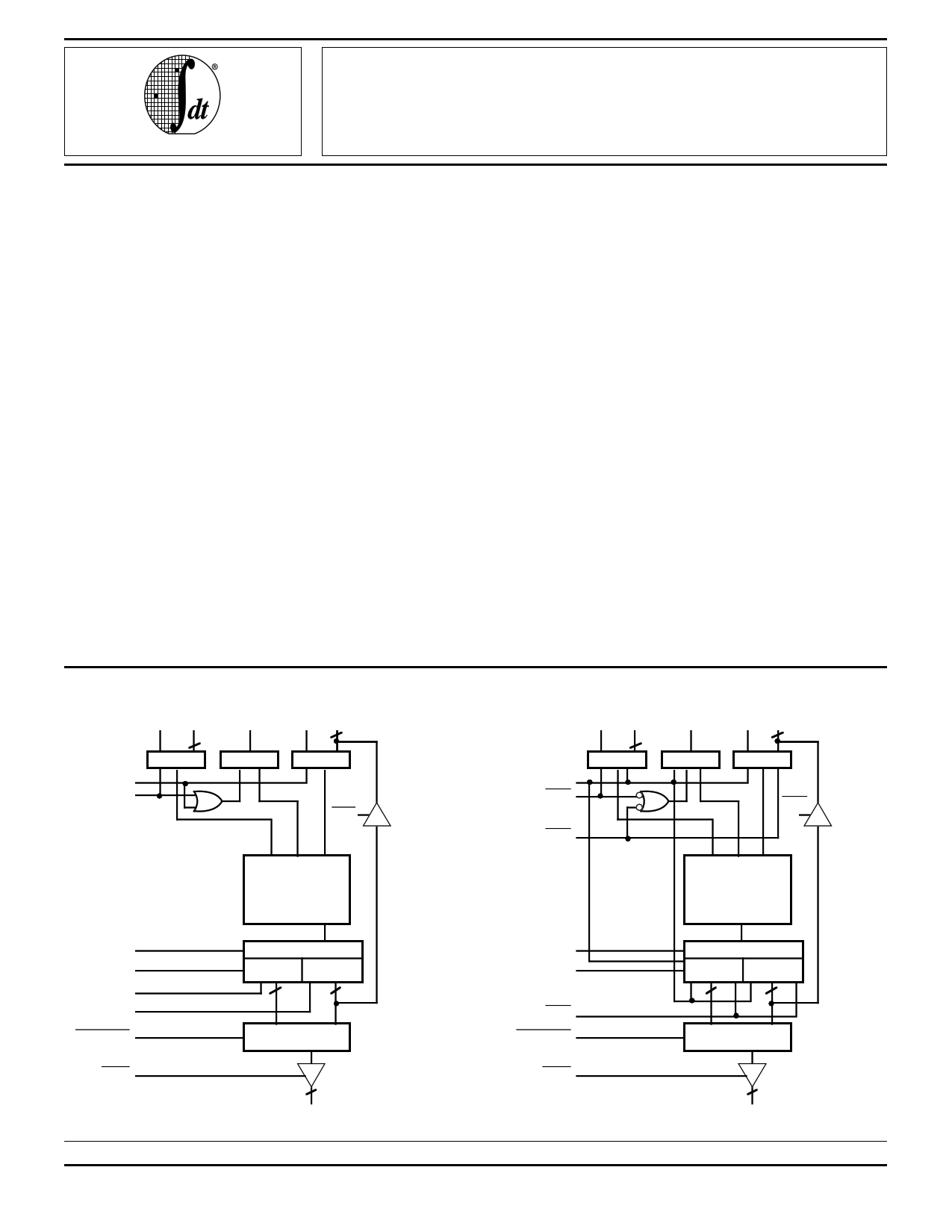
FUNCTIONAL BLOCK DIAGRAMS
IDT7216
XM X15-0
16
RND
YM Y15-0/P15-0
16
XREGISTER REGISTER YREGISTER
CLKY
CLKX
OEL
DESCRIPTION:
The IDT7216/IDT7217 are high-speed, low-power
16 x 16-bit multipliers ideal for fast, real time digital signal
processing applications. Utilization of a modified Booths
algorithm and IDT’s high-performance, submicron CMOS
technology, has achieved speeds comparable to bipolar (20ns
max.), at 1/10 the power consumption.
The IDT7216/IDT7217 are ideal for applications requiring
high-speed multiplication such as fast Fourier transform
analysis, digital filtering, graphic display systems, speech
synthesis and recognition and in any system requirement
where multiplication speeds of a mini/microcomputer are
inadequate.
All input registers, as well as LSP and MSP output regis-
ters, use the same positive edge-triggered D-type flip-flop. In
the IDT7216, there are independent clocks (CLKX, CLKY,
CLKM, CLKL) associated with each of these registers. The
IDT7217 has only a single clock input (CLK) and three register
enables. ENX and ENY control the two input registers, while
ENP controls the entire product.
The IDT7216/IDT7217 offer additional flexibility with the FA
control and MSPSEL functions. The FA control formats the
output for two’s complement by shifting the MSP up one bit
and then repeating the sign bit in the MSB of the LSP. The
CLK
ENX
IDT7217
XM X15-0 RND
16
XREGISTER
REGISTER
YM Y15-0/P15-0
16
YREGISTER
OEL
ENY
MULTIPLIER
ARRAY
MULTIPLIER
ARRAY
FA
FT
CLKM
CLKL
MSPSEL
FORMAT ADJUST
MSP
LSP
REGISTER REGISTER
16 16
MULTIPLEXER
OEP
16
PRODUCT
MSPOUT (P31 - P16)
The IDT Logo is a registered trademark of Integrated Device Technology, Inc.
2580 drw 01
MILITARY AND COMMERCIAL TEMPERATURE RANGES
©1995 Integrated Device Technology, Inc.
11.3
FA
FT
ENP
MSPSEL
OEP
FORMAT ADJUST
MSP
LSP
REGISTER REGISTER
16 16
MULTIPLEXER
16
PRODUCT
MSPOUT (P31 - P16) 2580 drw 02
AUGUST 1995
DSC-2023/6
1
1 page 
IDT7216L, IDT7217L
16 x 16 PARALLEL CMOS MULTIPLIERS
MILITARY AND COMMERCIAL TEMPERATURE RANGES
PIN DESCRIPTIONS
Pin Name
X0 - X15
Y0 - Y15/
P0 - P15
P16 - P31
OEL
OEP
XM, YM
RND
MSPSEL
FA
FT
CLK
CLKX
CLKY
CLKL
CLKM
ENX
ENY
I/O Description
I Data Inputs
I/O Y0 - Y15 are data inputs
P0 - P15 are LSP register output, enabled when OEL = 0
O Data Output (LSP or MSP)
I Output enable control for LSP (least significant product). When low enables P0 - P15. When high P0 - P15
tristated.
I Output enable control for MSP (most significant product). When low enables P16 - P31. When high P16 -
P31 tristated.
I Mode control for each data word. Low designates unsigned data input and high designates two's
complement.
I "Round" control for rounding of MSP. When high, 1 is added to the most significant bit of LSP. This
signal is affected by the state of FA pin. When FA = 1 and RND = 1, 1 is added to the 2-15 bit (P15). When
RND = 1 and FA = 0, 1 is added to the 2-16 bit (P14). The RND input is registered. It is clocked on the
rising edge of the logical OR of CLKX and CLKY in the 7216 and on the rising edge of CLK in the 7217.
Rounding always occurs in the positive direction which may introduce a systematic bias.
I When low, MSP is output on P16 - P31 lines. When high, LSP is output on P16 - P31.
I Format adjust control. When high, a full 32 bit product is selected. When low, a left shifted 31 bit product
is selected with the sign bit replicated in the LSP. FA is normally high, except for certain fractional two's
complement applications (see multiplier input / output formats).
I Flow through control. When high, both MSP and LSP registers are by-passed.
I 7217 X, Y, RND, LSP and MSP register clock input.
I 7216 X register clock input. Also clocks RND register.
I 7216 Y register clock input. Also clocks RND register.
I 7216 LSP register clock input.
I 7216 MSP register clock input.
I 7217 X register clock enable. Also enables RND register clock.
I 7217 Y register clock enable. Also enables RND register clock.
ABSOLUTE MAXIMUM RATINGS(1)
Symbol
Rating
Commercial Military Unit
VCC Power Supply –0.5 to +7.0 –0.5 to +7.0 V
Voltage
VTERM
Terminal Voltage
with Respect to
GND
VCC + 0.5
VCC + 0.5 V
TA Operating
0 to +70 –55 to +125 °C
Temperature
TBIAS Temperature
–55 to +125 –65 to +135 °C
Under Bias
TSTG Storage
–55 to +125 –65 to +150 °C
Temperature
IOUT
DC Output
50 50 mA
Current
NOTE:
2580 tbl 01
1. Stresses greater than those listed under ABSOLUTE MAXIMUM
RATINGS may cause permanent damage to the device. This is a stress
rating only and functional operation of the device at these or any other
conditions above those indicated in the operational sections of this
specification is not implied. Exposure to absolute maximum rating
conditions for extended periods may affect reliability.
CAPACITANCE (TA = +25°C, f = 1.0 MHz)
Symbol
Parameter(1)
Conditions Max. Unit
CIN Input Capacitance
VIN = 0V
10 pF
COUT Output Capacitance
VOUT = 0V
12 pF
NOTE:
2580 tbl 04
1. This parameter is measured at characterization and not tested.
11.3 5
5 Page 
IDT7216L, IDT7217L
16 x 16 PARALLEL CMOS MULTIPLIERS
MILITARY AND COMMERCIAL TEMPERATURE RANGES
11.3 11
11 Page | ||
| Páginas | Total 13 Páginas | |
| PDF Descargar | [ Datasheet IDT7217L.PDF ] | |
Hoja de datos destacado
| Número de pieza | Descripción | Fabricantes |
| IDT7217L | 16 x 16 PARALLEL CMOS MULTIPLIERS | Integrated Device Technology |
| Número de pieza | Descripción | Fabricantes |
| SLA6805M | High Voltage 3 phase Motor Driver IC. |
Sanken |
| SDC1742 | 12- and 14-Bit Hybrid Synchro / Resolver-to-Digital Converters. |
Analog Devices |
|
DataSheet.es es una pagina web que funciona como un repositorio de manuales o hoja de datos de muchos de los productos más populares, |
| DataSheet.es | 2020 | Privacy Policy | Contacto | Buscar |