|
|
PDF 74ACT299 Data sheet ( Hoja de datos )
| Número de pieza | 74ACT299 | |
| Descripción | 8-Input Universal Shift/Storage Register | |
| Fabricantes | Fairchild Semiconductor | |
| Logotipo | ||
Hay una vista previa y un enlace de descarga de 74ACT299 (archivo pdf) en la parte inferior de esta página. Total 11 Páginas | ||
|
No Preview Available !
July 1988
Revised November 1999
74AC299 • 74ACT299
8-Input Universal Shift/Storage Register
with Common Parallel I/O Pins
General Description
The AC/ACT299 is an 8-bit universal shift/storage register
with 3-STATE outputs. Four modes of operation are possi-
ble: hold (store), shift left, shift right and load data. The par-
allel load inputs and flip-flop outputs are multiplexed to
reduce the total number of package pins. Additional out-
puts are provided for flip-flops Q0, Q7 to allow easy serial
cascading. A separate active LOW Master Reset is used to
reset the register.
Features
s ICC and IOZ reduced by 50%
s Common parallel I/O for reduced pin count
s Additional serial inputs and outputs for expansion
s Four operating modes: shift left, shift right, load
and store
s 3-STATE outputs for bus-oriented applications
s Outputs source/sink 24 mA
s ACT299 has TTL-compatible inputs
Ordering Code:
Order Number Package Number
Package Description
74AC299SC
M20B
20-Lead Small Outline Integrated Circuit (SOIC), JEDEC MS-013, 0.300” Wide Body
74AC299SJ
M20D
20-Lead Small Outline Package (SOP), EIAJ TYPE II, 5.3mm Wide
74AC299MTC
MTC20
20-Lead Thin Shrink Small Outline Package (TSSOP), JEDEC MO-153, 4.4mm Wide
74AC299PC
N20A
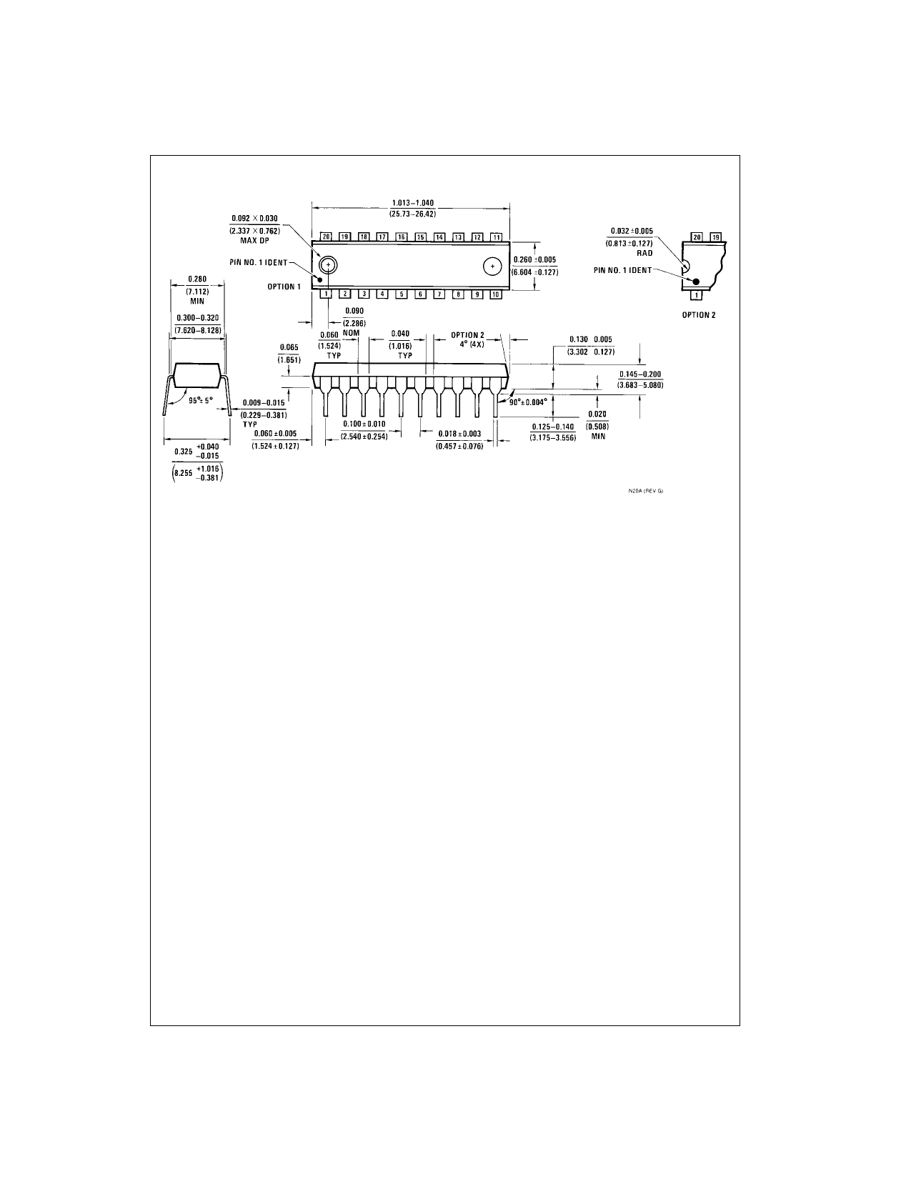
20-Lead Plastic Dual-In-Line Package (PDIP), JEDEC MS-001, 0.300” Wide
74ACT299SC
M20B
20-Lead Small Outline Integrated Circuit (SOIC), JEDEC MS-013, 0.300” Wide Body
74ACT299MTC
MTC20
20-Lead Thin Shrink Small Outline Package (TSSOP), JEDEC MO-153, 4.4mm Wide
74ACT299PC
N20A
20-Lead Plastic Dual-In-Line Package (PDIP), JEDEC MS-001, 0.300” Wide
Device also available in Tape and Reel. Specify by appending suffix letter “X” to the ordering code.
Connection Diagram
Pin Descriptions
Pin Names
CP
DS0
DS7
S0, S1
MR
OE1, OE2
I/O0–I/O7
Q0, Q7
Description
Clock Pulse Input
Serial Data Input for Right Shift
Serial Data Input for Left Shift
Mode Select Inputs
Asynchronous Master Reset
3-STATE Output Enable Inputs
Parallel Data Inputs or
3-STATE Parallel Outputs
Serial Outputs
FACT is a trademark of Fairchild Semiconductor Corporation.
© 1999 Fairchild Semiconductor Corporation DS009893
www.fairchildsemi.com
1 page 
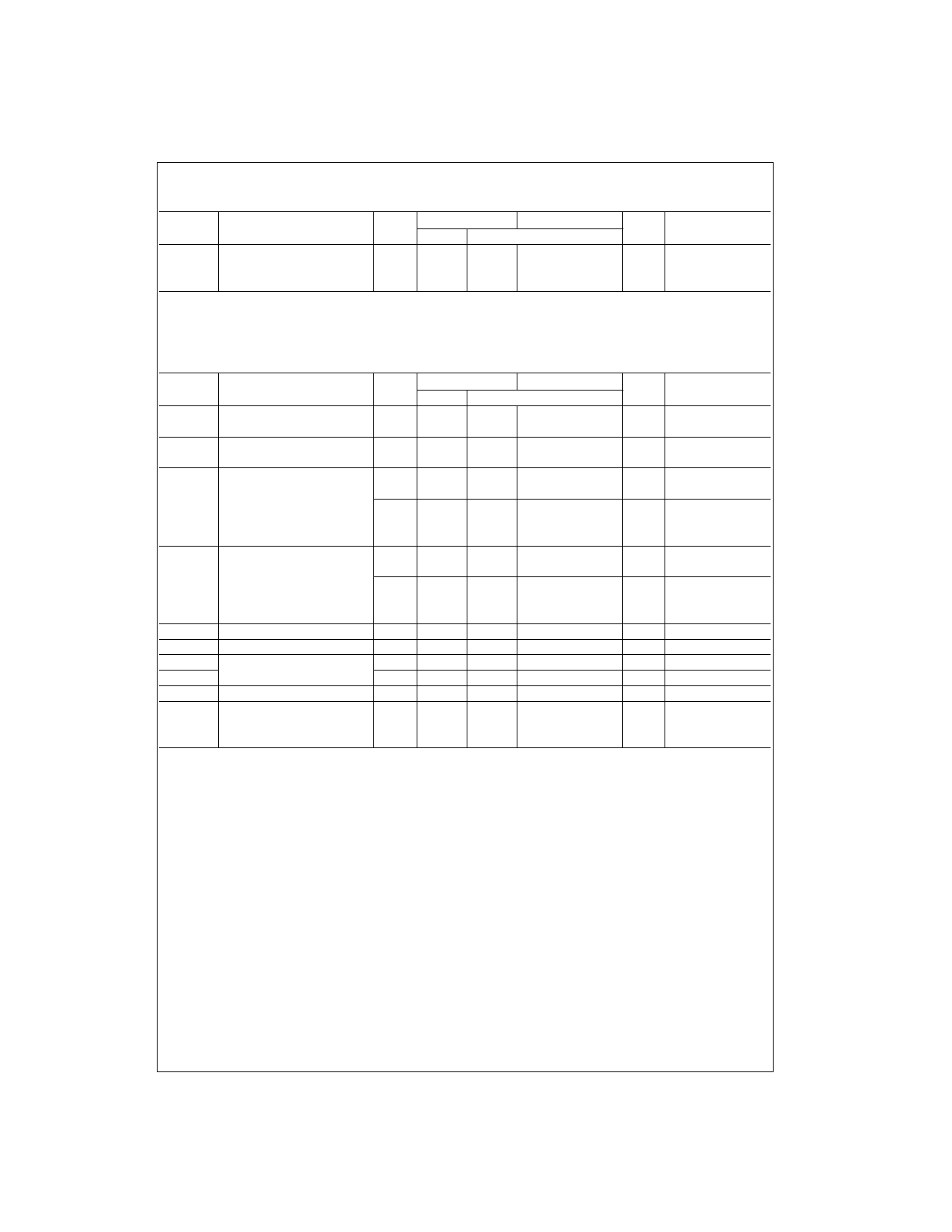
DC Electrical Characteristics for AC (Continued)
Symbol
Parameter
IOZT Maximum I/O Leakage Current
VCC
TA = 25°C
TA = −40°C to +85°C
(V) Typ
Guaranteed Limits
5.5
± 0.3
± 3.0
Note 2: All outputs loaded; threshold on input associated with output under test.
Note 3: Maximum test duration 20 ms, one output loaded at a time.
Note 4: IIN and ICC @ 3.0V are guaranteed to be less than or equal to the respective limit @ 5.5V VCC.
Units
Conditions
VI (OE) = VIL, VIH
µA VI = VCC, GND
VO = VCC, GND
DC Electrical Characteristics for ACT
Symbol
Parameter
VIH Minimum HIGH Level
Input Voltage
VIL Maximum LOW Level
Input Voltage
VOH Minimum HIGH Level
VCC
TA = 25°C
TA = −40°C to +85°C
(V) Typ
Guaranteed Limits
4.5 1.5
2.0
2.0
5.5 1.5
2.0
2.0
3.0 1.5
0.8
0.8
4.5 1.5
0.8
0.8
4.5 4.49
4.4
4.4
5.5 5.49
5.4
5.4
VOL Maximum LOW Level
Output Voltage
4.5 0.0001 3.86
5.5 4.86
4.5 0.001
0.1
5.5 0.001
0.1
3.76
4.76
0.1
0.1
IIN
ICCT
IOLD
IOHD
ICC
IOZT
4.5 0.36
5.5 0.36
Maximum Input Leakage Current
5.5
± 0.1
Maximum ICC/Input
Minimum Dynamic
5.5 0.6
5.5
Output Current (Note 6)
5.5
Maximum Quiescent Supply Current 5.5
4.0
Maximum I/O
Leakage Current
5.5 ±0.3
0.44
0.44
± 1.0
1.5
75
−75
40.0
±3.0
Note 5: All outputs loaded; thresholds on input associated with output under test.
Note 6: Maximum test duration 2.0 ms, one output loaded at a time.
Units
Conditions
V VOUT = 0.1V
or VCC − 0.1V
V VOUT = 0.1V
or VCC − 0.1V
V IOUT = −50 µA
VIN = VIL or VIH
V IOH = −24 mA
IOH = −24 mA (Note 5)
V IOUT = 50 µA
VIN = VIL or VIH
V IOL= 24 mA
IOL= 24 mA (Note 5)
µA VI = VCC, GND
mA VI = VCC − 2.1V
mA VOLD = 1.65V Max
mA VOHD = 3.85V Min
µA VIN = VCC or GND
VI (OE) = VIL, VIH
µA VI = VCC, GND
VO = VCC, GND
5 www.fairchildsemi.com
5 Page 
Physical Dimensions inches (millimeters) unless otherwise noted (Continued)
20-Lead Plastic Dual-In-Line Package (PDIP), JEDEC MS-001, 0.300” Wide
Package Number N20A
Fairchild does not assume any responsibility for use of any circuitry described, no circuit patent licenses are implied and
Fairchild reserves the right at any time without notice to change said circuitry and specifications.
LIFE SUPPORT POLICY
FAIRCHILD’S PRODUCTS ARE NOT AUTHORIZED FOR USE AS CRITICAL COMPONENTS IN LIFE SUPPORT
DEVICES OR SYSTEMS WITHOUT THE EXPRESS WRITTEN APPROVAL OF THE PRESIDENT OF FAIRCHILD
SEMICONDUCTOR CORPORATION. As used herein:
1. Life support devices or systems are devices or systems
which, (a) are intended for surgical implant into the
body, or (b) support or sustain life, and (c) whose failure
to perform when properly used in accordance with
instructions for use provided in the labeling, can be rea-
sonably expected to result in a significant injury to the
user.
2. A critical component in any component of a life support
device or system whose failure to perform can be rea-
sonably expected to cause the failure of the life support
device or system, or to affect its safety or effectiveness.
www.fairchildsemi.com
11 www.fairchildsemi.com
11 Page | ||
| Páginas | Total 11 Páginas | |
| PDF Descargar | [ Datasheet 74ACT299.PDF ] | |
Hoja de datos destacado
| Número de pieza | Descripción | Fabricantes |
| 74ACT299 | 8 BIT PIPO SHIFT REGISTER WITH ASYNCHRONOUS CLEAR | STMicroelectronics |
| 74ACT299 | 8-Input Universal Shift/Storage Register | Fairchild Semiconductor |
| 74ACT299B | 8 BIT PIPO SHIFT REGISTER WITH ASYNCHRONOUS CLEAR | STMicroelectronics |
| 74ACT299M | 8 BIT PIPO SHIFT REGISTER WITH ASYNCHRONOUS CLEAR | STMicroelectronics |
| Número de pieza | Descripción | Fabricantes |
| SLA6805M | High Voltage 3 phase Motor Driver IC. |
Sanken |
| SDC1742 | 12- and 14-Bit Hybrid Synchro / Resolver-to-Digital Converters. |
Analog Devices |
|
DataSheet.es es una pagina web que funciona como un repositorio de manuales o hoja de datos de muchos de los productos más populares, |
| DataSheet.es | 2020 | Privacy Policy | Contacto | Buscar |
