|
|
PDF EL7583 Data sheet ( Hoja de datos )
| Número de pieza | EL7583 | |
| Descripción | 3-Channel DC-DC Converter | |
| Fabricantes | Intersil Corporation | |
| Logotipo |  |
|
Hay una vista previa y un enlace de descarga de EL7583 (archivo pdf) en la parte inferior de esta página. Total 15 Páginas | ||
|
No Preview Available !
®
Data Sheet
July 24, 2003
EL7583
FN7335.2
3-Channel DC-DC Converter
The EL7583 is a 3-channel DC-DC
converter IC which is designed
primarily for use in TFT/LCD
applications. It features a PWM boost converter with 2.7V to
14V input capability and 5V to 17V output, which powers the
column drivers and provides up to 470mA @ 12V, 370mA @
15V from 5V supply. A pair of charge pump control circuits
provide regulated outputs of VON and VOFF supplies at 8V
to 40V and -5V to -40V, respectively, each at up to 60mA.
The EL7583 features adjustable switching frequency,
adjustable soft start, and a separate output VON enable
control to allow selection of supply start-up sequence. An
over-temperature feature is provided to allow the IC to be
automatically protected from excessive power dissipation.
The EL7583 is available in a 20-pin TSSOP package and is
specified for operation over the full -40°C to +85°C
temperature range.
Ordering Information
PART
NUMBER
EL7583IR
EL7583IR-T7
EL7583IR-T13
PACKAGE
20-Pin TSSOP
20-Pin TSSOP
20-Pin TSSOP
TAPE &
REEL
-
7”
13”
PKG. DWG. #
MDP0044
MDP0044
MDP0044
Features
• TFT/LCD display supply
- Boost regulator
- VON charge pump
- VOFF charge pump
• 2.7V to 14V VIN supply
• 5V < VBOOST < 17V
• 5V < VON < 40V
• -40V < VOFF < 0V
• VBOOST = 12V @ 470mA
• VBOOST = 15V @ 370mA
• High frequency, small inductor DC-DC boost circuit
• Over 90% efficient DC-DC boost converter capability
• Adjustable frequency
• Adjustable soft-start
• Adjustable outputs
• Small parts count
Applications
• TFT-LCD panels
• PDAs
Pinout
EL7583
(20-PIN TSSOP)
TOP VIEW
VSSB 1
SS 2
FBB 3
VDDB 4
LX 5
LX 6
LX 7
DRVN 8
VDDN 9
FBN 10
20 ROSC
19 ENP
18 ENBN
17 VREF
16 PGND
15 PGND
14 DRVP
13 VDDP
12 FBP
11 VSSP
REFER TO PCB LAYOUT GUIDELINE
1
CAUTION: These devices are sensitive to electrostatic discharge; follow proper IC Handling Procedures.
1-888-INTERSIL or 321-724-7143 | Intersil (and design) is a registered trademark of Intersil Americas Inc.
Copyright © Intersil Americas Inc. 2003. All Rights Reserved. Elantec is a registered trademark of Elantec Semiconductor, Inc.
All other trademarks mentioned are the property of their respective owners.
1 page 
EL7583
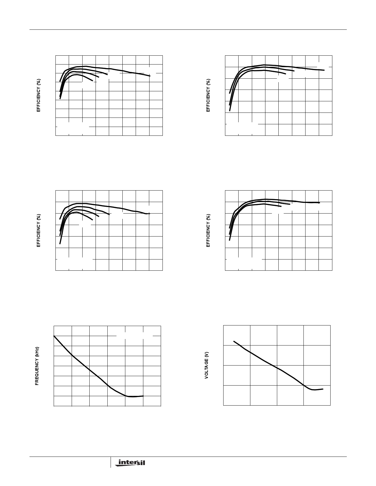
Typical Performance Curves
95
90
85 9V
80 15V 12V
75
5V
70
65
60
55 VIN=3.3V
FREQ=1MHz
50
0 100 200 300 400 500 600 700
IOUT (mA)
FIGURE 1. EFFICIENCY vs IOUT
800
95
90 9V
12V
85 15V
80
75
70
65 VIN=5V
FREQ=1MHz
60
0 100 200 300 400 500 600 700
IOUT (mA)
FIGURE 2. EFFICIENCY vs IOUT
800
95
90
5V
85 9V
80 15V 12V
75
70
65 VIN=3.3V
FREQ=700kHz
60
0 100 200 300 400 500 600 700
IOUT (mA)
FIGURE 3. EFFICIENCY vs IOUT
800
95
90
85
15V 12V
9V
80
75
70
65 VIN=5V
FREQ=700kHz
60
0 100 200 300 400 500 600 700
IOUT (mA)
FIGURE 4. EFFICIENCY vs IOUT
800
970
969
968
967
966
965
964
963
962
3
ROSC = 61.9kΩ
3.5 4 4.5 5
VDDB (V)
FIGURE 5. FS vs VDDB
5.5
6
1.27
1.265
1.26
1.255
1.25
-50
0 50 100
TEMPERATURE (°C)
FIGURE 6. VREF vs TEMPERATURE
150
5
5 Page 
Single Stage Charge Pump
EL7583
5V TO
17V
VOFF
VDDN
0.1µF
CCPN
COUT2
3.3µF
RONP
DRVN
RONN
VSSN
OSC
VDDP
RONP
DRVP
RONN
VSSP
0.1µF
CCPP
5V TO
17V
COUTV1ON
R12 2.2µF
R21 FBN
R22
VREF
FBP
+-
-+
+
-
VFBP
RON IS 30 - 40Ω FOR VDD 6V TO 12V
R11
Positive Charge Pump Design Considerations
A single stage charge pump is shown above. The maximum
VON output voltage is determined by the following equation:
VON(max) ≤ 2 × VDDCPP - IOUT × 2 × (RONN + RONP ) - 2 × VDIODE - IOUT × 0----.--5----×-----F----S--1---×-----C----C-----P----P- - IOUT × -0---.--5----×-----F----S----1-×-----C----O-----U----T----1-
where:
• RONN and RONP resistance values depend on the VDDP
voltage levels. For 12V supply, RON is typically 33Ω. For
6V supply, RON is typically 45Ω.
If additional stage is required, the LX switching signal is
recommended to drive the additional charge pump diodes.
The drive impedance at the LX switching is typically 150mΩ.
The figure below illustrates an implementation for two-stage
positive charge pump circuit.
11
11 Page | ||
| Páginas | Total 15 Páginas | |
| PDF Descargar | [ Datasheet EL7583.PDF ] | |
Hoja de datos destacado
| Número de pieza | Descripción | Fabricantes |
| EL7581 | 3-Channel DC-DC Converter | Intersil Corporation |
| EL7583 | 3-Channel DC-DC Converter | Intersil Corporation |
| EL7585 | TFT-LCD Power Supply | Intersil Corporation |
| EL7585A | TFT-LCD Power Supply | Intersil Corporation |
| Número de pieza | Descripción | Fabricantes |
| SLA6805M | High Voltage 3 phase Motor Driver IC. |
Sanken |
| SDC1742 | 12- and 14-Bit Hybrid Synchro / Resolver-to-Digital Converters. |
Analog Devices |
|
DataSheet.es es una pagina web que funciona como un repositorio de manuales o hoja de datos de muchos de los productos más populares, |
| DataSheet.es | 2020 | Privacy Policy | Contacto | Buscar |
