|
|
PDF HY29LV320TT-80 Data sheet ( Hoja de datos )
| Número de pieza | HY29LV320TT-80 | |
| Descripción | 32 Mbit (2M x 16) Low Voltage Flash Memory | |
| Fabricantes | Hynix Semiconductor | |
| Logotipo | ||
Hay una vista previa y un enlace de descarga de HY29LV320TT-80 (archivo pdf) en la parte inferior de esta página. Total 30 Páginas | ||
|
No Preview Available !
HY29LV320
32 Mbit (2M x 16) Low Voltage Flash Memory
KEY FEATURES
n Single Power Supply Operation
– Read, program and erase operations from
2.7 to 3.6 volts
– Ideal for battery-powered applications
n High Performance
– 70, 80, 90 and 120 ns access time
versions for full voltage range operation
n Ultra-low Power Consumption (Typical/
Maximum Values)
– Automatic sleep/standby current: 0.5/5.0
µA
– Read current: 9/16 mA (@ 5 MHz)
– Program/erase current: 20/30 mA
n Top and Bottom Boot Block Versions
– Provide one 8 KW, two 4 KW, one 16 KW
and sixty-three 32 KW sectors
n Secured Sector
– An extra 128-word, factory-lockable
sector available for an Electronic Serial
Number and/or additional secured data
n Sector Protection
– Allows locking of a sector or sectors to
prevent program or erase operations
within that sector
– Temporary Sector Unprotect allows
changes in locked sectors
n Fast Program and Erase Times (typicals)
– Sector erase time: 0.5 sec per sector
– Chip erase time: 32 sec
– Word program time: 11 µs
– Accelerated program time per word: 7 µs
n Automatic Erase Algorithm Preprograms
and Erases Any Combination of Sectors
or the Entire Chip
n Automatic Program Algorithm Writes and
Verifies Data at Specified Addresses
n Compliant With Common Flash Memory
Interface (CFI) Specification
– Flash device parameters stored directly
on the device
– Allows software driver to identify and use a
variety of current and future Flash products
n Minimum 100,000 Write Cycles per Sector
n Compatible With JEDEC standards
– Pinout and software compatible with
single-power supply Flash devices
– Superior inadvertent write protection
n Data# Polling and Toggle Bits
– Provide software confirmation of
completion of program and erase
operations
n Ready/Busy (RY/BY#) Pin
– Provides hardware confirmation of
completion of program and erase
operations
n Write Protect Function (WP#/ACC pin)
− Allows hardware protection of the first or
last 32 KW of the array, regardless of sector
protect status
n Acceleration Function (WP#/ACC pin)
− Provides accelerated program times
n Erase Suspend/Erase Resume
– Suspends an erase operation to allow
reading data from, or programming data
to, a sector that is not being erased
– Erase Resume can then be invoked to
complete suspended erasure
n Hardware Reset Pin (RESET#) Resets the
Device to Reading Array Data
n Space Efficient Packaging
– 48-pin TSOP and 63-ball FBGA packages
LOGIC DIAGRAM
21
A[20:0]
CE#
OE#
WE#
RESET#
DQ[15:0]
16
WP#/ACC
RY/BY#
Revision 1.3, May 2002
1 page 
PIN CONFIGURATIONS
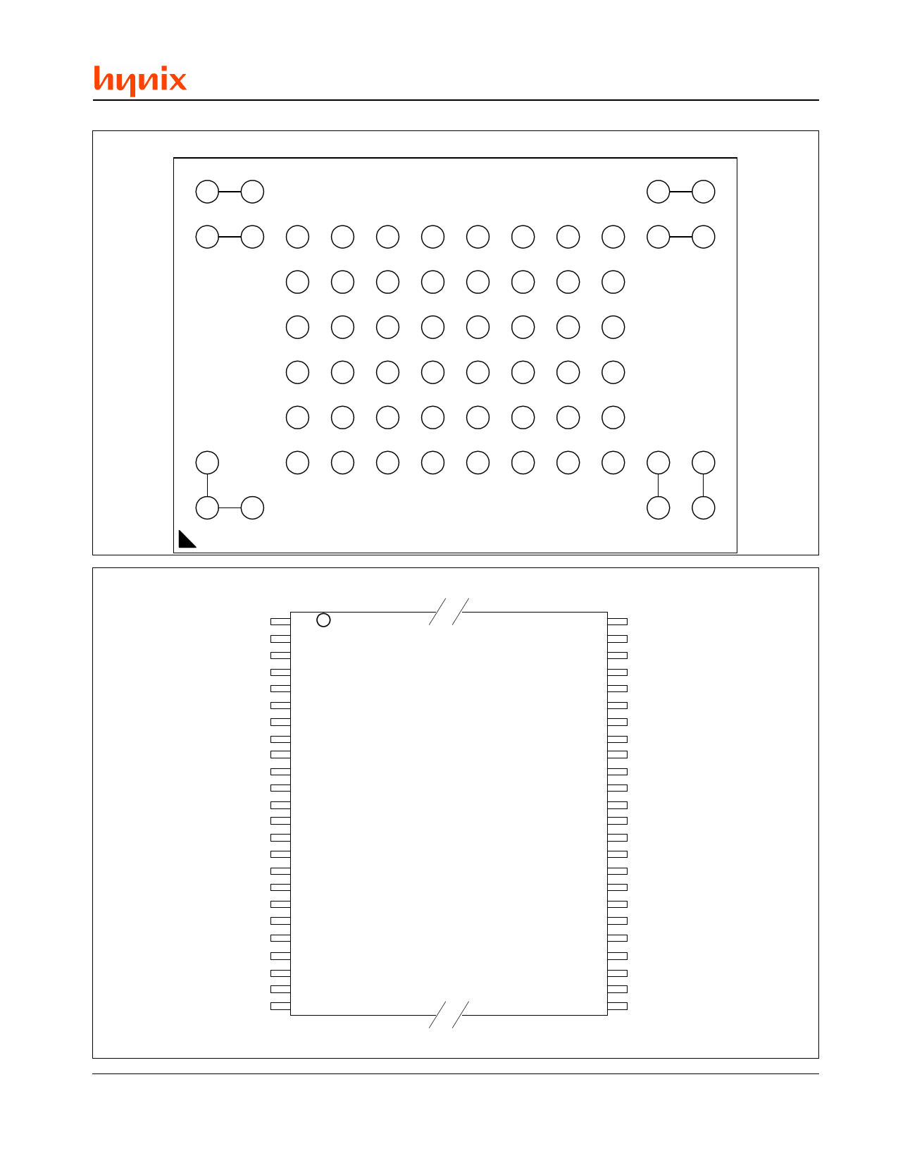
63- B allF B G A - To p V iew , B alls F acing D o w n
HY29LV320
A8 B8
NC NC
L8 M 8
NC NC
A 7 B 7 C 7 D 7 E 7 F7 G 7 H 7 J7 K 7 L7 M 7
N C N C A [13] A [12] A [14] A [15] A [16] V 10 D Q [15] V 55 N C N C
C 6 D 6 E 6 F6 G 6 H 6 J6 K 6
A [9] A [8] A [10] A [11] D Q [7] D Q [14] D Q [13] D Q [6]
C 5 D 5 E 5 F5 G 5 H 5 J5 K 5
W E # R E S E T# N C A [19] D Q [5] D Q [12] V + + D Q [4]
C 4 D 4 E 4 F4 G 4 H 4 J4 K 4
R Y /B Y # W P # /A C C A [18] A [20] D Q [2] D Q [10] D Q [11] D Q [3]
C3 D3 E3
A [7] A [17] A [6]
F3 G 3 H 3 J3 K 3
A [5] D Q [0] D Q [8] D Q [9] D Q [1]
A 2 C 2 D 2 E 2 F2 G 2 H 2 J2 K 2 L2 M 2
NC
A [3] A [4] A [2] A [1] A [0] C E # O E #
V55
NC
NC
A1 B1
L1 M 1
NC NC
NC NC
A[15]
A[14]
A[13]
A[12]
A[11]
A[10]
A[9]
A[8]
A[19]
A[20]
WE#
RESET#
NC
WP#/ACC
RY/BY#
A[18]
A[17]
A[7]
A[6]
A[5]
A[4]
A[3]
A[2]
A[1]
1
2
3
4
5
6
7
8
9
10
11
12
13
14
15
16
17
18
19
20
21
22
23
24
r1.3/May 02
TSOP48
48 A[16]
47 VIH
46 VSS
45 DQ[15]
44 DQ[7]
43 DQ[14]
42 DQ[6]
41 DQ[13]
40 DQ[5]
39 DQ[12]
38 DQ[4]
37 VCC
36 DQ[11]
35 DQ[3]
34 DQ[10]
33 DQ[2]
32 DQ[9]
31 DQ[1]
30 DQ[8]
29 DQ[0]
28 OE#
27 VSS
26 CE#
25 A[0]
5
5 Page 
HY29LV320
WE#
OE#
ADR
ADR
CE#
OE#
DATA OUT
tACC
tCE
tOE
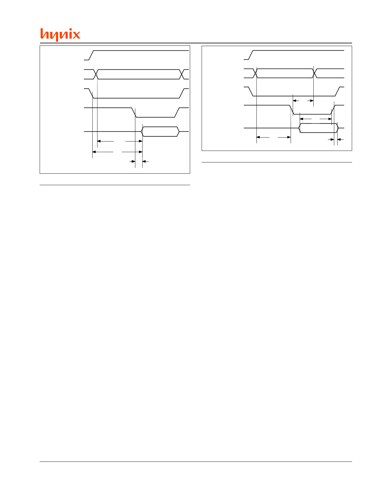
Figure 1. Read Operation
Write Operation
Certain operations, including programming data
and erasing sectors of memory, require the host
to write a command or command sequence to the
HY29LV320. Writes to the device are performed
by placing the word address on the device’s ad-
dress inputs while the data to be written is input
on DQ[15:0]. The host system must drive the CE#
and WE# pins Low and drive OE# High for a valid
write operation to take place. All addresses are
latched on the falling edge of WE# or CE#, which-
ever happens later. All data is latched on the ris-
ing edge of WE# or CE#, whichever happens first.
See Figure 2.
.The “Device Commands” section of this specifi-
cation provides details on the specific device com-
mands implemented in the HY29LV320.
Accelerated Program Operation
This device offers accelerated program operations
through the “Accelerate” function provided by the
WP#/ACC pin. This function is intended primarily
for faster programming throughput at the factory.
If VHH is applied to the WP#/ACC input, the device
enters the Unlock Bypass mode, temporarily
unprotects any protected sectors, and uses the
higher voltage on the pin to reduce the time re-
quired for program operations. The system would
then use the two-cycle program command se-
quence as required by the Unlock Bypass mode.
Removing VHH from the pin returns the device to
normal operation.
CE#
WE#
DATA IN
tAH
tDS
tAS
tDH
Figure 2. Write Operation
Note: WP# sector protection cannot be used while WP#/
ACC = VHH. Thus, all sectors are unprotected and can
be erased and programmed while in Accelerated Pro-
gramming mode.
Note: The Accelerate function does not affect the time
required for Erase operations.
See the description of the WP#/ACC pin in the
Pin Descriptions table for additional information
on this function.
Write Protect Function
The Write Protect function provides a hardware
method of protecting the boot sectors without us-
ing VID. This function is a second function pro-
vided by the WP#/ACC pin.
Placing this pin at VIL disables program and erase
operations in the bottom or top 32K words of the
array (the boot sectors). The affected sectors are
as follows (see Tables 1 and 2):
n HY29LV320B: S0 – S3
n HY29LV320T: S63 – S66
If the pin is placed at VIH, the protection state of
those sectors reverts to whether they were last
set to be protected or unprotected using the
method described in the Sector Group Protection
and Unprotection sections.
Note: Sectors protected by WP#/ACC = V remain pro-
IL
tected during Temporary Sector Unprotect and cannot
be erased or programmed. Also see note under Accel-
erate Program Operation above.
Standby Operation
When the system is not reading or writing to the
device, it can place the device in the Standby
r1.3/May 02
11
11 Page | ||
| Páginas | Total 30 Páginas | |
| PDF Descargar | [ Datasheet HY29LV320TT-80.PDF ] | |
Hoja de datos destacado
| Número de pieza | Descripción | Fabricantes |
| HY29LV320TT-80 | 32 Mbit (2M x 16) Low Voltage Flash Memory | Hynix Semiconductor |
| HY29LV320TT-80I | 32 Mbit (2M x 16) Low Voltage Flash Memory | Hynix Semiconductor |
| Número de pieza | Descripción | Fabricantes |
| SLA6805M | High Voltage 3 phase Motor Driver IC. |
Sanken |
| SDC1742 | 12- and 14-Bit Hybrid Synchro / Resolver-to-Digital Converters. |
Analog Devices |
|
DataSheet.es es una pagina web que funciona como un repositorio de manuales o hoja de datos de muchos de los productos más populares, |
| DataSheet.es | 2020 | Privacy Policy | Contacto | Buscar |
