|
|
|
PDF HY29LV160TT-70 Data sheet ( Hoja de datos )
| Número de pieza | HY29LV160TT-70 | |
| Descripción | 16 Mbit (2M x 8/1M x 16) Low Voltage Flash Memory | |
| Fabricantes | Hynix Semiconductor | |
| Logotipo | ||
Hay una vista previa y un enlace de descarga de HY29LV160TT-70 (archivo pdf) en la parte inferior de esta página. Total 30 Páginas | ||
|
No Preview Available !
HY29LV160
16 Mbit (2M x 8/1M x 16) Low Voltage Flash Memory
KEY FEATURES
n Single Power Supply Operation
– Read, program and erase operations from
2.7 to 3.6 volts
– Ideal for battery-powered applications
n High Performance
– 70, 80, 90 and 120 ns access time
versions
n Ultra-low Power Consumption (Typical
Values At 5 Mhz)
– Automatic sleep mode current: 1 µA
– Standby mode current: 1 µA
– Read current: 9 mA
– Program/erase current: 20 mA
n Flexible Sector Architecture:
– One 16 KB, two 8 KB, one 32 KB and
thirty-one 64 KB sectors in byte mode
– One 8 KW, two 4 KW, one 16 KW and
thirty-one 32 KW sectors in word mode
– Top or bottom boot block configurations
available
n Sector Protection
– Allows locking of a sector or sectors to
prevent program or erase operations
within that sector
– Sectors lockable in-system or via
programming equipment
– Temporary Sector Unprotect allows
changes in locked sectors (requires high
voltage on RESET# pin)
n Fast Program and Erase Times
– Sector erase time: 0.25 sec typical for
each sector
– Chip erase time: 8 sec typical
– Byte program time: 9 µs typical
n Unlock Bypass Program Command
– Reduces programming time when issuing
multiple program command sequences
n Automatic Erase Algorithm Preprograms
and Erases Any Combination of Sectors
or the Entire Chip
n Erase Suspend/Erase Resume
– Suspends an erase operation to allow
reading data from, or programming data
to, a sector that is not being erased
– Erase Resume can then be invoked to
complete suspended erasure
n Automatic Program Algorithm Writes and
Verifies Data at Specified Addresses
n 100,000 Write Cycles per Sector Minimum
n Data# Polling and Toggle Bits
– Provide software confirmation of
completion of program and erase
operations
n Ready/Busy# Pin
– Provides hardware confirmation of
completion of program and erase
operations
n Hardware Reset Pin (RESET#) Resets the
Device to Reading Array Data
n Compliant With Common Flash Memory
Interface (CFI) Specification
– Flash device parameters stored directly
on the device
– Allows software driver to identify and use
a variety of different current and future
Flash products
n Compatible With JEDEC standards
– Pinout and software compatible with
single-power supply Flash devices
– Superior inadvertent write protection
n Space Efficient Packaging
– 48-pin TSOP and 48-ball FBGA packages
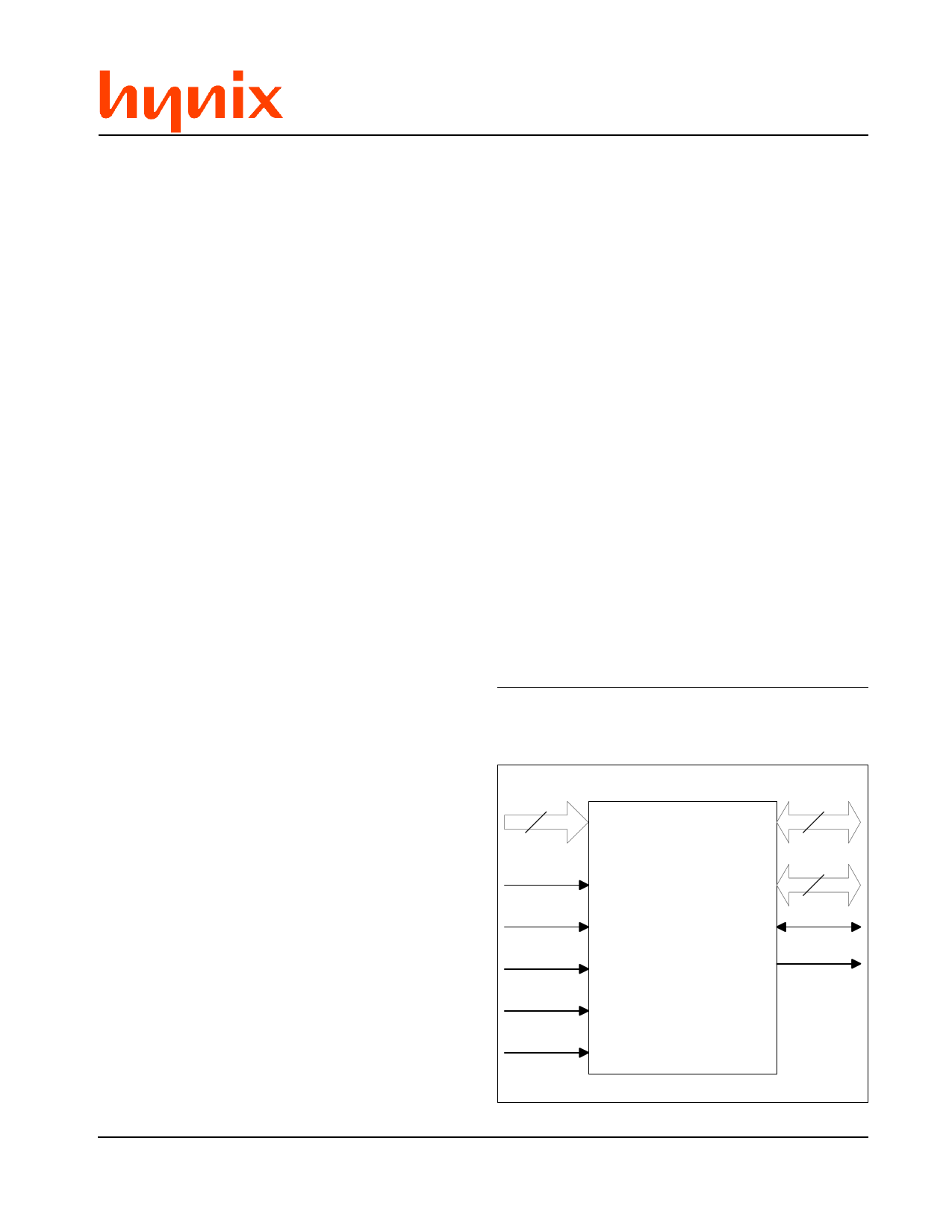
LOGIC DIAGRAM
20
A[19:0]
CE#
OE#
WE#
RESET#
BYTE#
DQ[7:0]
DQ[14:8]
DQ15/A-1
RY/BY#
8
7
Preliminary
Revision 1.2, May 2001
1 page 
CONVENTIONS
Unless otherwise noted, a positive logic (active
High) convention is assumed throughout this docu-
ment, whereby the presence at a pin of a higher,
more positive voltage (VIH) causes assertion of the
signal. A ‘#’ symbol following the signal name, e.g.,
RESET#, indicates that the signal is asserted in
the Low state (VIL). See DC specifications for VIH
and VIL values.
MEMORY ARRAY ORGANIZATION
The 16 Mbit Flash memory array is organized into
35 blocks called sectors (S0, S1, . . . , S34). A
sector is the smallest unit that can be erased and
that can be protected to prevent accidental or un-
authorized erasure. See the ‘Bus Operations’ and
‘Command Definitions’ sections of this document
for additional information on these functions.
In the HY29LV160, four of the sectors, which com-
prise the boot block, vary in size from 8 to 32
BUS OPERATIONS
Device bus operations are initiated through the
internal command register, which consists of sets
of latches that store the commands, along with
the address and data information, if any, needed
to execute the specific command. The command
register itself does not occupy any addressable
memory location. The contents of the command
register serve as inputs to an internal state ma-
chine whose outputs control the operation of the
device. Table 3 lists the normal bus operations,
the inputs and control levels they require, and the
resulting outputs. Certain bus operations require
a high voltage on one or more device pins. Those
are described in Table 4.
Read Operation
Data is read from the HY29LV160 by using stan-
dard microprocessor read cycles while placing the
byte or word address on the device’s address in-
puts. The host system must drive the CE# and
OE# pins LOW and drive WE# high for a valid
read operation to take place. The BYTE# pin de-
termines whether the device outputs array data in
words (DQ[15:0]) or in bytes (DQ[7:0]).
The HY29LV160 is automatically set for reading
array data after device power-up and after a hard-
HY29LV160
Whenever a signal is separated into numbered
bits, e.g., DQ[7], DQ[6], ..., DQ[0], the family of
bits may also be shown collectively, e.g., as
DQ[7:0].
The designation 0xNNNN (N = 0, 1, 2, . . . , 9, A, .
. . , E, F) indicates a number expressed in hexadeci-
mal notation. The designation 0bXXXX indicates a
number expressed in binary notation (X = 0, 1).
Kbytes (4 to 16 Kwords), while the remaining 31
sectors are uniformly sized at 64 Kbytes (32
Kwords). The boot block can be located at the
bottom of the address range (HY29LV160B) or at
the top of the address range (HY29LV160T).
Tables 1 and 2 define the sector addresses and
corresponding address ranges for the top and bot-
tom boot block versions of the HY29LV160.
ware reset to ensure that no spurious alteration of
the memory content occurs during the power tran-
sition. No command is necessary in this mode to
obtain array data, and the device remains enabled
for read accesses until the command register con-
tents are altered.
This device features an Erase Suspend mode.
While in this mode, the host may read the array
data from any sector of memory that is not marked
for erasure. If the host reads from an address
within an erase-suspended (or erasing) sector, or
while the device is performing a byte or word pro-
gram operation, the device outputs status data
instead of array data. After completing an Auto-
matic Program or Automatic Erase algorithm within
a sector, that sector automatically returns to the
read array data mode. After completing a program-
ming operation in the Erase Suspend mode, the
system may once again read array data with the
same exception noted above.
The host must issue a hardware reset or the soft-
ware reset command to return a sector to the read
array data mode if DQ[5] goes high during a pro-
gram or erase cycle, or to return the device to the
read array data mode while it is in the Electronic
ID mode.
Rev. 1.2/May 01
5
5 Page 
START
(Note: All sectors must be
protected prior to
unprotecting any sector)
TRYCNT = 1
SNUM = 0
RESET# = VID
Wait 1 us
Write 0x60 to device
Set Address:
A[6] = 1, A]1] = 1, A]0] = 0
Write 0x60 to Address
Wait 15 ms
HY29LV160
Set Address:
A[19:12] = Sector SNUM
A[6] = 1, A]1] = 1, A]0] = 0
Write 0x40 to Address
Read from Address
Data = 0x00?
NO
TRYCNT = 1000? YES
YES
SNUM = 34?
YES
NO
SNUM = SNUM + 1
NO
Increment TRYCNT
RESET# = VIH
Write Reset Command
SECTOR UNPROTECT
COMPLETE
DEVICE FAILURE
Figure 2. Sector Unprotect Algorithm
START
RESET# = VID
(All protected sectors
become unprotected)
Perform Program or Erase
Operations
RESET# = VIH
(All previously protected
sectors return to protected
state)
TEMPORARY SECTOR
UNPROTECT COMPLETE
Figure 3. Temporary Sector Unprotect
Algorithm
Electronic ID Operation (High Voltage Method)
The Electronic ID mode provides manufacturer and
device identification and sector protection verifi-
cation through codes output on DQ[15:0]. This
mode is intended primarily for programming equip-
ment to automatically match a device to be pro-
grammed with its corresponding programming al-
gorithm.
Two methods are provided for accessing the Elec-
tronic ID data. The first requires VID on address
pin A[9], with additional requirements for obtain-
ing specific data items listed in Table 4. The Elec-
tronic ID data can also be obtained by the host
through specific commands issued via the com-
mand register, as described in the ‘Device Com-
mands’ section of this data sheet.
While in the high-voltage Electronic ID mode, the
system may read at specific addresses to obtain
certain device identification and status informa-
tion:
A read cycle at address 0xXXX00 retrieves the
manufacturer code.
A read cycle at address 0xXXX01 in Word
mode or 0xXXX02 in Byte mode returns the
device code.
A read cycle containing a sector address (SA)
in A[19:12] and the address 0x02 in Word mode
or 0x04 in Byte mode, returns 0x01 if that sec-
tor is protected, or 0x00 if it is unprotected.
Rev. 1.2/May 01
11
11 Page | ||
| Páginas | Total 30 Páginas | |
| PDF Descargar | [ Datasheet HY29LV160TT-70.PDF ] | |
Hoja de datos destacado
| Número de pieza | Descripción | Fabricantes |
| HY29LV160TT-70 | 16 Mbit (2M x 8/1M x 16) Low Voltage Flash Memory | Hynix Semiconductor |
| HY29LV160TT-70I | 16 Mbit (2M x 8/1M x 16) Low Voltage Flash Memory | Hynix Semiconductor |
| Número de pieza | Descripción | Fabricantes |
| SLA6805M | High Voltage 3 phase Motor Driver IC. |
Sanken |
| SDC1742 | 12- and 14-Bit Hybrid Synchro / Resolver-to-Digital Converters. |
Analog Devices |
|
DataSheet.es es una pagina web que funciona como un repositorio de manuales o hoja de datos de muchos de los productos más populares, |
| DataSheet.es | 2020 | Privacy Policy | Contacto | Buscar |