|
|
|
PDF 5962-9688401QXA Data sheet ( Hoja de datos )
| Número de pieza | 5962-9688401QXA | |
| Descripción | 1A Low Dropout Regulator for 5V to 3.3V Conversion | |
| Fabricantes | National Semiconductor | |
| Logotipo | ||
Hay una vista previa y un enlace de descarga de 5962-9688401QXA (archivo pdf) en la parte inferior de esta página. Total 11 Páginas | ||
|
No Preview Available !
May 1999
LM3940
1A Low Dropout Regulator for 5V to 3.3V Conversion
General Description
The LM3940 is a 1A low dropout regulator designed to pro-
vide 3.3V from a 5V supply.
The LM3940 is ideally suited for systems which contain both
5V and 3.3V logic, with prime power provided from a 5V bus.
Because the LM3940 is a true low dropout regulator, it can
hold its 3.3V output in regulation with input voltages as low
as 4.5V.
The T0-220 package of the LM3940 means that in most ap-
plications the full 1A of load current can be delivered without
using an additional heatsink.
The surface mount TO-263 package uses minimum board
space, and gives excellent power dissipation capability when
soldered to a copper plane on the PC board.
Features
n Output voltage specified over temperature
n Excellent load regulation
n Guaranteed 1A output current
n Requires only one external component
n Built-in protection against excess temperature
n Short circuit protected
Applications
n Laptop/Desktop Computers
n Logic Systems
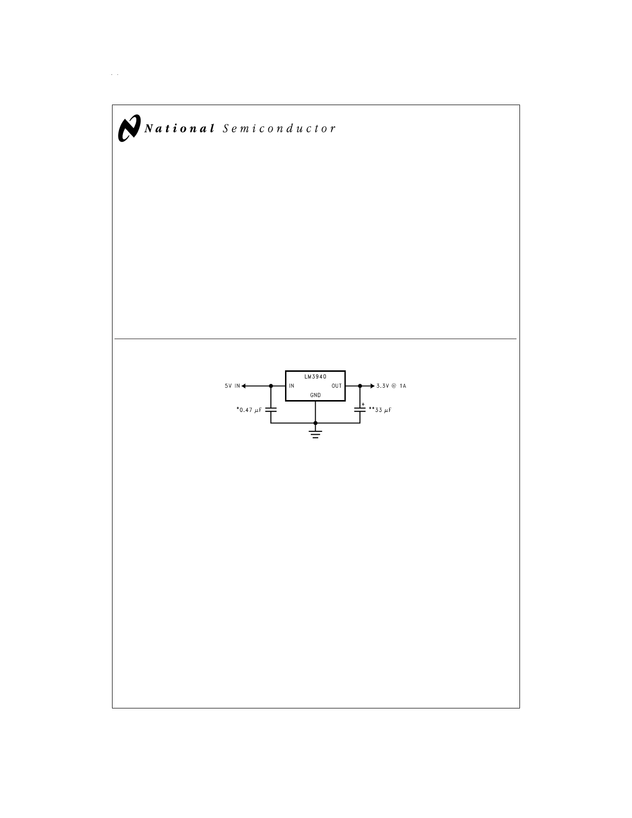
Typical Application
DS012080-1
*Required if regulator is located more than 1" from the power supply filter capacitor or if battery power is used.
**See Application Hints.
© 1999 National Semiconductor Corporation DS012080
www.national.com
1 page 
Application Hints
EXTERNAL CAPACITORS
The output capacitor is critical to maintaining regulator stabil-
ity, and must meet the required conditions for both ESR
(Equivalent Series Resistance) and minimum amount of ca-
pacitance.
MINIMUM CAPACITANCE:
The minimum output capacitance required to maintain stabil-
ity is 33 µF (this value may be increased without limit).
Larger values of output capacitance will give improved tran-
sient response.
ESR LIMITS:
The ESR of the output capacitor will cause loop instability if
it is too high or too low. The acceptable range of ESR plotted
versus load current is shown in the graph below. It is essen-
tial that the output capacitor meet these requirements,
or oscillations can result.
DS012080-5
FIGURE 1. ESR Limits
It is important to note that for most capacitors, ESR is speci-
fied only at room temperature. However, the designer must
ensure that the ESR will stay inside the limits shown over the
entire operating temperature range for the design.
For aluminum electrolytic capacitors, ESR will increase by
about 30X as the temperature is reduced from 25˚C to
−40˚C. This type of capacitor is not well-suited for low tem-
perature operation.
Solid tantalum capacitors have a more stable ESR over tem-
perature, but are more expensive than aluminum electrolyt-
ics. A cost-effective approach sometimes used is to parallel
an aluminum electrolytic with a solid Tantalum, with the total
capacitance split about 75/25% with the Aluminum being the
larger value.
If two capacitors are paralleled, the effective ESR is the par-
allel of the two individual values. The “flatter” ESR of the Tan-
talum will keep the effective ESR from rising as quickly at low
temperatures.
HEATSINKING
A heatsink may be required depending on the maximum
power dissipation and maximum ambient temperature of the
application. Under all possible operating conditions, the junc-
tion temperature must be within the range specified under
Absolute Maximum Ratings.
To determine if a heatsink is required, the power dissipated
by the regulator, PD, must be calculated.
The figure below shows the voltages and currents which are
present in the circuit, as well as the formula for calculating
the power dissipated in the regulator:
DS012080-6
IIN = IL + IG
PD = (VIN − VOUT) IL + (VIN) IG
FIGURE 2. Power Dissipation Diagram
The next parameter which must be calculated is the maxi-
mum allowable temperature rise, TR (max). This is calcu-
lated by using the formula:
TR (max) = TJ (max) − TA (max)
Where: TJ (max) is the maximum allowable junction tem-
perature, which is 125˚C for commercial
grade parts.
TA (max)
is the maximum ambient temperature
which will be encountered in the applica-
tion.
Using the calculated values for TR(max) and PD, the maxi-
mum allowable value for the junction-to-ambient thermal re-
sistance, θ(J−A), can now be found:
θ(J−A) = TR (max)/PD
IMPORTANT: If the maximum allowable value for θ(J−A) is
found to be ≥ 60˚C/W for the TO-220 package, ≥ 80˚C/W for
the TO-263 package, or ≥174˚C/W for the SOT-223 pack-
age, no heatsink is needed since the package alone will dis-
sipate enough heat to satisfy these requirements.
If the calculated value for θ(J−A)falls below these limits, a
heatsink is required.
HEATSINKING TO-220 PACKAGE PARTS
The TO-220 can be attached to a typical heatsink, or se-
cured to a copper plane on a PC board. If a copper plane is
to be used, the values of θ(J−A) will be the same as shown in
the next section for the TO-263.
5 www.national.com
5 Page 
Physical Dimensions inches (millimeters) unless otherwise noted (Continued)
16-Lead Ceramic Surface-Mount Package
Order Part Number LM3940WG-3.3-QML
5962-9688401QXA
NSC Package Number WG16A
LIFE SUPPORT POLICY
NATIONAL’S PRODUCTS ARE NOT AUTHORIZED FOR USE AS CRITICAL COMPONENTS IN LIFE SUPPORT
DEVICES OR SYSTEMS WITHOUT THE EXPRESS WRITTEN APPROVAL OF THE PRESIDENT AND GENERAL
COUNSEL OF NATIONAL SEMICONDUCTOR CORPORATION. As used herein:
1. Life support devices or systems are devices or
systems which, (a) are intended for surgical implant
into the body, or (b) support or sustain life, and
whose failure to perform when properly used in
accordance with instructions for use provided in the
labeling, can be reasonably expected to result in a
significant injury to the user.
2. A critical component is any component of a life
support device or system whose failure to perform
can be reasonably expected to cause the failure of
the life support device or system, or to affect its
safety or effectiveness.
National Semiconductor
Corporation
Americas
Tel: 1-800-272-9959
Fax: 1-800-737-7018
Email: [email protected]
www.national.com
National Semiconductor
Europe
Fax: +49 (0) 1 80-530 85 86
Email: [email protected]
Deutsch Tel: +49 (0) 1 80-530 85 85
English Tel: +49 (0) 1 80-532 78 32
Français Tel: +49 (0) 1 80-532 93 58
Italiano Tel: +49 (0) 1 80-534 16 80
National Semiconductor
Asia Pacific Customer
Response Group
Tel: 65-2544466
Fax: 65-2504466
Email: [email protected]
National Semiconductor
Japan Ltd.
Tel: 81-3-5639-7560
Fax: 81-3-5639-7507
National does not assume any responsibility for use of any circuitry described, no circuit patent licenses are implied and National reserves the right at any time without notice to change said circuitry and specifications.
11 Page | ||
| Páginas | Total 11 Páginas | |
| PDF Descargar | [ Datasheet 5962-9688401QXA.PDF ] | |
Hoja de datos destacado
| Número de pieza | Descripción | Fabricantes |
| 5962-9688401QXA | 1A Low Dropout Regulator for 5V to 3.3V Conversion | National Semiconductor |
| Número de pieza | Descripción | Fabricantes |
| SLA6805M | High Voltage 3 phase Motor Driver IC. |
Sanken |
| SDC1742 | 12- and 14-Bit Hybrid Synchro / Resolver-to-Digital Converters. |
Analog Devices |
|
DataSheet.es es una pagina web que funciona como un repositorio de manuales o hoja de datos de muchos de los productos más populares, |
| DataSheet.es | 2020 | Privacy Policy | Contacto | Buscar |