|
|
|
PDF 5962-9313301MPA Data sheet ( Hoja de datos )
| Número de pieza | 5962-9313301MPA | |
| Descripción | Ultralow Distortion/ Ultralow Noise Op Amp | |
| Fabricantes | Analog Devices | |
| Logotipo | ||
Hay una vista previa y un enlace de descarga de 5962-9313301MPA (archivo pdf) en la parte inferior de esta página. Total 16 Páginas | ||
|
No Preview Available !
a
FEATURES
Low Noise
0.9 nV/√Hz typ (1.2 nV/√Hz max) Input Voltage
Noise at 1 kHz
50 nV p-p Input Voltage Noise, 0.1 Hz to 10 Hz
Low Distortion
–120 dB Total Harmonic Distortion at 20 kHz
Excellent AC Characteristics
800 ns Settling Time to 16 Bits (10 V Step)
110 MHz Gain Bandwidth (G = 1000)
8 MHz Bandwidth (G = 10)
280 kHz Full Power Bandwidth at 20 V p-p
20 V/s Slew Rate
Excellent DC Precision
80 V max Input Offset Voltage
1.0 V/؇C VOS Drift
Specified for ؎5 V and ؎15 V Power Supplies
High Output Drive Current of 50 mA
APPLICATIONS
Professional Audio Preamplifiers
IR, CCD, and Sonar Imaging Systems
Spectrum Analyzers
Ultrasound Preamplifiers
Seismic Detectors
⌺⌬ ADC/DAC Buffers
PRODUCT DESCRIPTION
The AD797 is a very low noise, low distortion operational
amplifier ideal for use as a preamplifier. The low noise of
0.9 nV/√Hz and low total harmonic distortion of –120 dB at
audio bandwidths give the AD797 the wide dynamic range
5
Ultralow Distortion,
Ultralow Noise Op Amp
AD797*
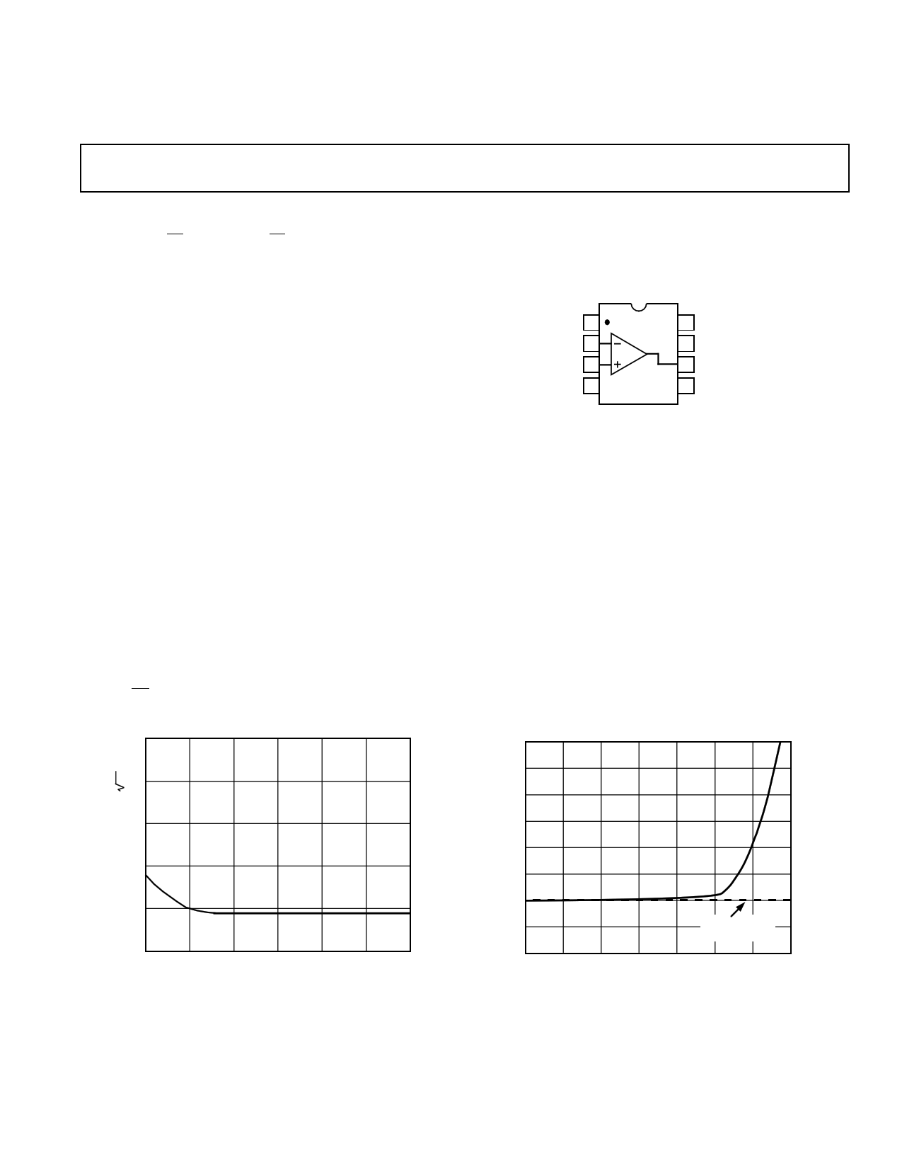
CONNECTION DIAGRAM
8-Pin Plastic Mini-DIP (N),
Cerdip (Q) and SOIC (R) Packages
OFFSET NULL 1
–IN 2
+IN 3
–VS 4
AD797
TOP VIEW
DECOMPENSATION &
DISTORTION
8 NEUTRALIZATION
7 +VS
6 OUTPUT
5 OFFSET NULL
necessary for preamps in microphones and mixing consoles.
Furthermore, the AD797’s excellent slew rate of 20 V/µs and
110 MHz gain bandwidth make it highly suitable for low fre-
quency ultrasound applications.
The AD797 is also useful in IR and Sonar Imaging applications
where the widest dynamic range is necessary. The low distor-
tion and 16-bit settling time of the AD797 make it ideal for
buffering the inputs to Σ∆ ADCs or the outputs of high resolu-
tion DACs especially when they are used in critical applications
such as seismic detection and spectrum analyzers. Key features
such as a 50 mA output current drive and the specified power
supply voltage range of ± 5 to ± 15 volts make the AD797 an
excellent general purpose amplifier.
–90
4
–100
0.001
3
–110
0.0003
2
1
0
10
100
1k
10k 100k
1M
FREQUENCY – Hz
AD797 Voltage Noise Spectral Density
*Patent pending.
10M
REV. C
Information furnished by Analog Devices is believed to be accurate and
reliable. However, no responsibility is assumed by Analog Devices for its
use, nor for any infringements of patents or other rights of third parties
which may result from its use. No license is granted by implication or
otherwise under any patent or patent rights of Analog Devices.
–120
–130
100
300
MEASUREMENT
LIMIT
0.0001
1k 3k 10k 30k
FREQUENCY – Hz
THD vs. Frequency
100k 300k
One Technology Way, P.O. Box 9106, Norwood, MA 02062-9106, U.S.A.
Tel: 617/329-4700
Fax: 617/326-8703
1 page 
11
10 +125°C
9
8 +25°C
7
–55°C
6
0 5 10 15 20
SUPPLY VOLTAGE – ±Volts
Figure 7. Quiescent Supply Current vs. Supply Voltage
12
FREQ = 1kHz
RL = 600Ω
G = +10
9
6
3
AD797
140
120
PSR
PSR
+SUPPLY
100 –SUPPLY
150
80 125
CMR
60 100
40 75
20
1
50
10 100 1k 10k 100k 1M
FREQUENCY – Hz
Figure 10. Power Supply and Common-Mode Rejection
vs. Frequency
–60
RL = 600 Ω
G = +10
FREQ = 10kHz
NOISE BW = 100kHz
–80
–100
VS = ±5V
VS = ±15V
0
0 ±5 ±10 ±15 ±20
SUPPLY VOLTAGE – Volts
Figure 8. Output Voltage vs. Supply for 0.01% Distortion
1.0
0.8
0.0015%
0.6
0.01%
0.4
0.2
–120
0.01
0.1
1.0
10
OUTPUT LEVEL – Volts
Figure 11. Total Harmonic Distortion (THD) + Noise vs.
Output Level
30
±15V SUPPLIES
20
RL = 600 Ω
10
±5V SUPPLIES
0.0
0 2 4 6 8 10
STEP SIZE – Volts
Figure 9. Settling Time vs. Step Size (±)
0
10k 100k 1M 10M
Figure 12. Large Signal Frequency Response
REV. C
–5–
5 Page 
AD797
20–120pF
100 Ω
R1
IIN
CS*
+VS
27
AD797
34
RS*
–VS
**
6
**
VOUT
600Ω
* SEE TEXT
** USE POWER SUPPLY BYPASSING SHOWN IN FIGURE 32.
Figure 36. I-to-V Converter Connection
greater than 33 pF a 100 Ω series resistor is required. A by-
passed balancing resistor (RS and CS) can be included to mini-
mize dc errors.
THE INVERTING CONFIGURATION
The inverting configuration (Figure 37) presents a low input
impedance, R1, to the source. For this reason, the goals of both
low noise and input buffering are at odds with one another.
Nonetheless, the excellent dynamics of the AD797 will make it
the preferred choice in many inverting applications, and with care-
ful selection of feedback resistors the noise penalties will be mini-
mal. Some examples are presented in Table II and Figure 37.
CL
R2
R1
VIN
RS*
+VS
**
27
AD797
34
6
**
–VS
VOUT
RL
* SEE TEXT
** USE POWER SUPPLY BYPASSING SHOWN IN FIGURE 32.
Figure 37. Inverting Amplifier Connection
Gain
–1
–1
–10
Table III. Values for Inverting Circuit
R1
1 kΩ
300 Ω
150 Ω
R2
1 kΩ
300 Ω
1500 Ω
CL
≈20 pF
≈10 pF
≈5 pF
Noise
(Excluding rS)
3.0 nV/√Hz
1.8 nV/√Hz
1.8 nV/√Hz
DRIVING CAPACITIVE LOADS
The capacitive load driving capabilities of the AD797 are dis-
played in Figure 38. At gains over 10 usually no special precau-
tions are necessary. If more drive is desirable the circuit in
Figure 39 should be used. Here a 5000 pF load can be driven
cleanly at any noise gain ≥ 2.
100nF
10nF
1nF
100pF
10pF
1pF
1
10 100
CLOSED-LOOP GAIN
1k
Figure 38. Capacitive Load Drive Capability vs. Closed
Loop Gain
20pF
1k Ω
VIN
1k Ω
200pF
100 Ω
+VS
**
27
AD797
34
6
**
33Ω
VOUT
C1
–VS
** USE POWER SUPPLY BYPASSING SHOWN IN FIGURE 32.
Figure 39. Recommended Circuit for Driving a High
Capacitance Load
SETTLING TIME
The AD797 is unique among ultralow noise amplifiers in that it
settles to 16 bits (<150 µV) in less than 800 ns. Measuring this
performance presents a challenge. A special test setup (Figure
40) was developed for this purpose. The input signal was ob-
tained from a resonant reed switch pulse generator, available
from Tektronix as calibration Fixture No. 067-0608-00. When
open, the switch is simply 50 Ω to ground and settling is purely
a passive pulse decay and inherently flat. The low repetition rate
signal was captured on a digital oscilloscope after being ampli-
fied and clamped twice. The selection of plug-in for the oscillo-
scope was made for minimum overload recovery.
REV. C
–11–
11 Page | ||
| Páginas | Total 16 Páginas | |
| PDF Descargar | [ Datasheet 5962-9313301MPA.PDF ] | |
Hoja de datos destacado
| Número de pieza | Descripción | Fabricantes |
| 5962-9313301MPA | Ultralow Distortion/ Ultralow Noise Op Amp | Analog Devices |
| Número de pieza | Descripción | Fabricantes |
| SLA6805M | High Voltage 3 phase Motor Driver IC. |
Sanken |
| SDC1742 | 12- and 14-Bit Hybrid Synchro / Resolver-to-Digital Converters. |
Analog Devices |
|
DataSheet.es es una pagina web que funciona como un repositorio de manuales o hoja de datos de muchos de los productos más populares, |
| DataSheet.es | 2020 | Privacy Policy | Contacto | Buscar |