|
|
|
PDF E142AHF Data sheet ( Hoja de datos )
| Número de pieza | E142AHF | |
| Descripción | Per Pin timing Deskew w 4x2 Cross Point Switch | |
| Fabricantes | Semtech Corporation | |
| Logotipo | ||
Hay una vista previa y un enlace de descarga de E142AHF (archivo pdf) en la parte inferior de esta página. Total 19 Páginas | ||
|
No Preview Available !
EDGE HIGH-PERFORMANCE PRODUCTS
Description
Edge142
Per Pin timing Deskew w 4x2
Cross Point Switch
Features
The Edge142 is a 4 X 2 cross point switch with output
edge deskew capability. Manufactured in a high
performance bipolar process, it is designed primarily for
channel deskew applications in VLSI and Mixed-Signal
test equipment.
Any of the four input signals may be selected as the
source for either output. The 142 performs test head
multiplexing, adjacent channel multiplexing, and signal
buffering for both the drive and receive signals, in addition
to timing deskew.
• Very Narrow (<1 ns) Pulse Width Capability
• Fmax > 850 MHz
• Independent Delay Adjustments for Positive and
Negative Transitions
• Delay Range of 1.5 ns
• Trailing Edge Adjust Range of 300 ps
• Small Footprint: 52-pin MQFP Package
(10 X 10 mm) with Internal Heat Spreader or
Die Form
The delay value (and resolution) is controlled via an
external voltage DAC. The delay element is designed
specifically to be monotonic and very stable while
delaying a very narrow pulse over a limited delay range.
Applications
The part offers separate delays for rising vs. falling edges.
The rising edge delay range is 1.5 ns and the falling
edge adjustment range is 300 ps.
The Edge142 is also well suited for 1:2 or 1:4 signal
fanout applications that require:
- multiple signal sources
- output enable / disable
- timing deskew on the output
signals.
• Automatic Test Equipment
– Per pin deskew in VLSI, Mixed-Signal, and Memory
Testers
– Clock Distribution with timing adjustment
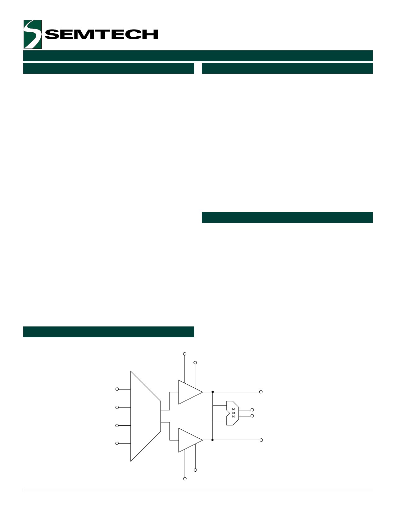
Functional Block Diagram
VDELAY 0
VFALL 0
IN0 / 0*
IN1 / 1*
IN2 / 2*
IN3 / 3*
4X2
∆T
∆T
OUT0 / 0*
MUX OUT0 / 0*
MUX OUT1 / 1*
OUT1 / 1*
Revision 1, February 14, 2000
VFALL 1
VDELAY 1
1
www.semtech.com
1 page 
Edge142
EDGE HIGH-PERFORMANCE PRODUCTS
Circuit Description (continued)
Input Multiplexer
Output Enable
The Edge142 offers a 4 X 2 cross point switch in which
one of four input signals are selected to two independent
outputs. Each output signal’s propagation delay and
pulse width may then be adjusted via external control.
Both the output and multiplexer output signals may be
enabled or disabled, as documented below.
EN* OUT/OUT* MUX EN MUX(0,1)OUT
The truth table below documents the multiplexer
functionality. Notice that there are no restrictions
between the selection of channel 0 and channel 1.
0 Active
10
Propagation Delay Adjust
0
1
0
Active
SEL01 SEL00 OUT0 SEL11 SEL10 OUT1
0
0 IN0 0
0 IN0
0
1 IN1 0
1 IN1
The Edge142 supports two independent delay functions,
which are described in the table below.
1
0 IN2 1
0 IN2
Tpd+
Tpd-
1
1 IN3 1
1 IN3
VDELAY
1.5 ns
1.5 ns
Output Multiplexer
The Edge142 provides MUX OUT0 / MUX OUT0* and
MUX OUT1 / MUX OUT1*, additional buffered differential
output signals. These signals are selected from OUT0
or OUT1, depending on the state of MUX SEL, as indicated
in the table below.
MUX(0,1) SEL MUXOUT0
MUXOUT1
0 OUT0 / OUT0* OUT1 / OUT1*
VFALL 0 ps 300 ps
VDELAY controls the propagation delay of both the rising
and falling edge (see Figure 2). An input signal is
selected and then delayed by some programmable
amount (Tspan) determined by the analog input VDELAY.
The rising and falling edges are delayed equally. The
propagation delay for a rising and a falling edge is defined
as
Tpd+, Tpd- = Tpd(nom) + Tspan
1 OUT1 / OUT1* OUT0 / OUT0*
The MUX OUT signals allow either of the delayed outputs
to be sent to an alternative destination without having
to daisy chain the outputs to multiple destinations. This
feature permits point to point routing of all critical timing
signals in an effort to maintain the cleanest transmission
lines for these signals.
The MUX OUT signals also provide a method for sending
one common selected input signal to two independent
destinations. This feature is useful when fanning out
driver data and driver enable signals to multiple test
heads.
where Tpd(nom) is the propagation delay of the part
with zero programmed delay, and Tspan is the additional
delay programmed via the VDELAY input. Notice that
Tspan can be either positive or negative, depending on
the nominal biasing of VDELAY, thus allowing bidirectional
propagation delay adjustment. The transfer function
for Tspan vs. VDELAY is shown in Figure 4.
INPUT
TPD min
TPD min
OUTPUT
(VDELAY = +0.1V)
OUTPUT
(VDELAY = –1.3V)
Tspan
Tspan
2000 Semtech Corp.
Figure 2. VDELAY Control
5 www.semtech.com
5 Page 
Edge142
EDGE HIGH-PERFORMANCE PRODUCTS
Application Information (continued)
Temperature Coefficient
The propagation delay temperature coefficient is shown
in the above two charts. The same information is
displayed on two different scales to enhance readability.
The 142 functions over the entire VDELAY voltage range,
but the timing error due to changes in the ambient
temperature becomes large for VDELAY < -1.1V. If
extreme accuracy is required, the recommended voltage
range is: +0.1V >= VDELAY >= -1.1V. If greater range is
needed and thermal drift can be tolerated, or the ambient
temperature is very tightly controlled, the entire voltage
range may be used.
Edge 142 Temperature Coefficient vs. VDELAY
vs. Ambient
60
50
40
30
20
10
0
-0.1
-0.4
-0.8
-1.1
VDELAY [V]
-1.3
Tpd+ 30-40°C
Tpd- 30-40°C
Tpd+ 40-50°C
Tpd- 40-50°C
Tpd+ 50-60°C
Tpd- 50-60°C
Edge 142 Temperature Coefficient vs. VDELAY
vs. Ambient
6
5
4
3
2
1
0
-0.1
-0.4
-0.8
-1.1
VDELAY [V]
-1.3
Tpd+ 30-40°C
Tpd- 30-40°C
Tpd+ 40-50°C
Tpd- 40-50°C
Tpd+ 50-60°C
Tpd- 50-60°C
2000 Semtech Corp.
11 www.semtech.com
11 Page | ||
| Páginas | Total 19 Páginas | |
| PDF Descargar | [ Datasheet E142AHF.PDF ] | |
Hoja de datos destacado
| Número de pieza | Descripción | Fabricantes |
| E142AHF | Per Pin timing Deskew w 4x2 Cross Point Switch | Semtech Corporation |
| Número de pieza | Descripción | Fabricantes |
| SLA6805M | High Voltage 3 phase Motor Driver IC. |
Sanken |
| SDC1742 | 12- and 14-Bit Hybrid Synchro / Resolver-to-Digital Converters. |
Analog Devices |
|
DataSheet.es es una pagina web que funciona como un repositorio de manuales o hoja de datos de muchos de los productos más populares, |
| DataSheet.es | 2020 | Privacy Policy | Contacto | Buscar |