|
|
|
PDF DS5002FPM-16 Data sheet ( Hoja de datos )
| Número de pieza | DS5002FPM-16 | |
| Descripción | Secure Microprocessor Chip | |
| Fabricantes | Dallas Semiconducotr | |
| Logotipo | ||
Hay una vista previa y un enlace de descarga de DS5002FPM-16 (archivo pdf) en la parte inferior de esta página. Total 25 Páginas | ||
|
No Preview Available !
www.maxim-ic.com
GENERAL DESCRIPTION
The DS5002FP secure microprocessor chip is a
secure version of the DS5001FP 128k soft
microprocessor chip. In addition to the memory and
I/O enhancements of the DS5001FP, the secure
microprocessor chip incorporates the most
sophisticated security features available in any
processor. The security features of the DS5002FP
include an array of mechanisms that are designed to
resist all levels of threat, including observation,
analysis, and physical attack. As a result, a massive
effort is required to obtain any information about
memory contents. Furthermore, the “soft” nature of
the DS5002FP allows frequent modification of the
secure information, thereby minimizing the value of
any secure information obtained by such a massive
effort.
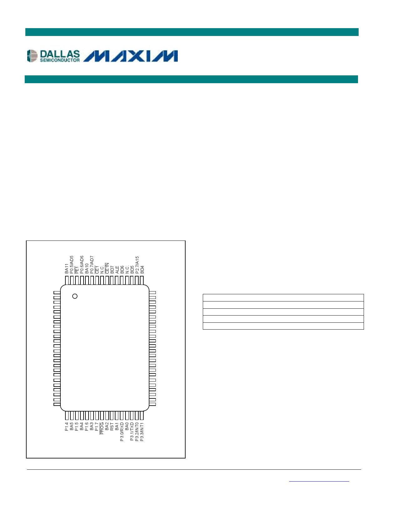
PIN CONFIGURATION
TOP VIEW
P0.4AD4
CE2
PE2
BA9
P0.3/AD3
BA8
P0.2/AD2
BA13
P0.1/AD1
R/W
P0.0/AD0
VCC0
VCC
MSEL
P1.0
BA14
P1.1
BA12
P1.2
BA7
P1.3
PE3
PE4
BA6
80 79 78 77 76 75 74 73 72 71 70 69 68 67 66 65
1 64
2 63
3 62
4 61
5 60
6
7
Dallas
59
58
8
9
Semiconductor
57
56
10 DS5002FP 55
11 54
12 53
13 52
14 51
15 50
16 49
17 48
18 47
19 46
20 45
21 44
22 43
23 42
24 41
25 26 27 28 29 30 31 32 33 34 35 36 37 38 39 40
P2.6/A14
CE3
CE4
BD3
P2.5/A13
BD2
P2.4/A12
BD1
P2.3/A11
BD0
VLI
SDI
GND
P2.2/A10
P2.1/A9
P2.0/A8
XTAL1
XTAL2
P3.7/RD
P3.6/WR
P3.5/TI
PF
VRST
P3.4/T0
DS5002FP
Secure Microprocessor Chip
FEATURES
§ 8051-Compatible Microprocessor for
Secure/Sensitive Applications
Access 32kB, 64kB, or 128kB of NV SRAM for
Program and/or Data Storage
In-System Programming Through On-Chip Serial
Port
Can Modify Its Own Program or Data Memory in
the End System
§ Firmware Security Features
Memory Stored in Encrypted Form
Encryption Using On-Chip 64-Bit Key
Automatic True Random Key Generator
Self Destruct Input (SDI)
Optional Top Coating Prevents Microprobe
(DS5002FPM)
Improved Security Over Previous Generations
Protects Memory Contents from Piracy
§ Crash-Proof Operation
Maintains All Nonvolatile Resources for Over 10
Years in the Absence of Power
Power-Fail Reset
Early Warning Power-Fail Interrupt
Watchdog Timer
ORDERING INFORMATION
PART
TEMP RANGE PIN-PACKAGE
DS5002FP-16
0°C to +70°C
80 QFP
DS5002FPM-16
0°C to +70°C
80 QFP
DS5002FP-16N
-40°C to +85°C 80 QFP
DS5002FMN-16 -40°C to +85°C 80 QFP
Selector Guide appears at end of data sheet.
QFP
Note: Some revisions of this device may incorporate deviations from published specifications known as errata. Multiple revisions of any device
may be simultaneously available through various sales channels. For information about device errata, click here: www.maxim-ic.com/errata.
1 of 25
REV: 030503
1 page 
Figure 2. Expanded Data Memory Write Cycle
DS5002FP Secure Microprocessor Chip
AC CHARACTERISTICS—EXTERNAL CLOCK DRIVE
(VCC = 5V ± 10%, TA = 0°C to +70°C.) (Figure 3)
# PARAMETER SYMBOL
28 External Clock High Time
tCLKHPW
29 External Clock Low Time
tCLKLPW
30 External Clock Rise Time
tCLKR
31 External Clock Fall Time
tCLKF
CONDITIONS
12MHz
16MHz
12MHz
16MHz
12MHz
16MHz
12MHz
16MHz
Figure 3. External Clock Timing
MIN MAX UNITS
20
15
ns
20
15
ns
20
15
ns
20
15
ns
5 of 25
5 Page 
DS5002FP Secure Microprocessor Chip
PIN DESCRIPTION
PIN
11, 9, 7, 5,
1, 79, 77,
75
15, 17, 19,
21, 25, 27,
29, 31
49, 50, 51,
56, 58, 60,
64, 66
36
38
39
40
41
44
45
46
34
70
47, 48
52
13
12
54
16, 8, 18,
80, 76, 4, 6,
20, 24, 26,
28, 30, 33,
35, 37
71, 69, 67,
65,
61, 59, 57,
55
10
74
2
63
NAME
P0.0–P0.7
P1.0–P1.7
P2.0–P2.7
P3.0 RXD
P3.1 TXD
P3.2 INT0
P3.3 INT1
P3.4 T0
P3.5 T1
P3.6 WR
P3.7 RD
RST
ALE
XTAL2, XTAL1
GND
VCC
VCCO
VLI
BA14–0
BD7–0
R/W
CE1
CE2
CE3
FUNCTION
General-Purpose I/O Port 0. This port is open-drain and cannot drive a logic 1. It requires
external pullups. Port 0 is also the multiplexed expanded address/data bus. When used in
this mode, it does not require pullups.
General-Purpose I/O Port 1
General-Purpose I/O Port 2. Also serves as the MSB of the expanded address bus.
General-Purpose I/O Port Pin 3.0. Also serves as the receive signal for the on-board UART.
This pin should not be connected directly to a PC COM port.
General-Purpose I/O Port Pin 3.1. Also serves as the transmit signal for the on-board UART.
This pin should not be connected directly to a PC COM port.
General-Purpose I/O Port Pin 3.2. Also serves as the active-low external interrupt 0.
General-Purpose I/O Port Pin 3.3. Also serves as the active-low external interrupt 1.
General-Purpose I/O Port Pin 3.4. Also serves as the timer 0 input.
General-Purpose I/O Port Pin 3.5. Also serves as the timer 1 input.
General-Purpose I/O Port Pin. Also serves as the write strobe for Expanded bus operation.
General-Purpose I/O Port Pin. Also serves as the read strobe for Expanded bus operation.
Active-High Reset Input. A logic 1 applied to this pin activates a reset state. This pin is pulled
down internally so this pin can be left unconnected if not used. An RC power-on reset circuit
is not needed and is not recommended.
Address Latch Enable. Used to demultiplex the multiplexed expanded address/data bus on
port 0. This pin is normally connected to the clock input on a ’373 type transparent latch.
XTAL1, XTAL 2. Used to connect an external crystal to the internal oscillator. XTAL1 is the
input to an inverting amplifier and XTAL2 is the output.
Logic Ground
VCC - +5V
VCCO - VCC Output. This is switched between VCC and VLI by internal circuits based on the
level of VCC. When power is above the lithium input, power is drawn from VCC. The lithium cell
remains isolated from a load. When VCC is below VLI, the VCCO switches to the VLI source.
VCCO should be connected to the VCC pin of an SRAM.
Lithium Voltage Input. Connect to a lithium cell greater than VLIMIN and no greater than VLIMAX
as shown in the electrical specifications. Nominal value is +3V.
Byte-Wide Address Bus Bits 14–0. This bus is combined with the nonmultiplexed data bus
(BD7–0) to access NV SRAM. Decoding is performed using CE1 through CE4 . Therefore,
BA15 is not actually needed. Read/write access is controlled by R/ W . BA14–0 connect
directly to an 8k, 32k, or 128k SRAM. If an 8k RAM is used, BA13 and BA14 are
unconnected. If a 128k SRAM is used, the micro converts CE2 and CE3 to serve as A16 and
A15, respectively.
Byte-Wide Data Bus Bits 7–0. This 8-bit bidirectional bus is combined with the
nonmultiplexed address bus (BA14–0) to access NV SRAM. Decoding is performed on CE1
and CE2. Read/write access is controlled by R/W. D7–0 connect directly to an SRAM, and
optionally to a real-time clock or other peripheral.
Read/Write. This signal provides the write enable to the SRAMs on the byte-wide bus. It is
controlled by the memory map and partition. The blocks selected as program (ROM) are
write-protected.
Chip Enable 1. This is the primary decoded chip enable for memory access on the byte-wide
bus. It connects to the chip-enable input of one SRAM. CE1 is lithium-backed. It remains in a
logic-high inactive state when VCC falls below VLI.
Chip Enable 2. This chip enable is provided to access a second 32k block of memory. It
connects to the chip-enable input of one SRAM. When MSEL = 0, the micro converts CE2
into A16 for a 128k x 8 SRAM. CE2 is lithium-backed and remains at a logic high when VCC
falls below VLI.
Chip Enable 3. This chip enable is provided to access a third 32k block of memory. It
connects to the chip enable input of one SRAM. When MSEL = 0, the micro converts CE3
11 of 25
11 Page | ||
| Páginas | Total 25 Páginas | |
| PDF Descargar | [ Datasheet DS5002FPM-16.PDF ] | |
Hoja de datos destacado
| Número de pieza | Descripción | Fabricantes |
| DS5002FPM-16 | Secure Microprocessor Chip | Dallas Semiconducotr |
| Número de pieza | Descripción | Fabricantes |
| SLA6805M | High Voltage 3 phase Motor Driver IC. |
Sanken |
| SDC1742 | 12- and 14-Bit Hybrid Synchro / Resolver-to-Digital Converters. |
Analog Devices |
|
DataSheet.es es una pagina web que funciona como un repositorio de manuales o hoja de datos de muchos de los productos más populares, |
| DataSheet.es | 2020 | Privacy Policy | Contacto | Buscar |