|
|
PDF DS2404 Data sheet ( Hoja de datos )
| Número de pieza | DS2404 | |
| Descripción | EconoRAM Time Chip | |
| Fabricantes | Dallas Semiconducotr | |
| Logotipo | ||
Hay una vista previa y un enlace de descarga de DS2404 (archivo pdf) en la parte inferior de esta página. Total 29 Páginas | ||
|
No Preview Available !
DS2404
EconoRAM Time Chip
www.maxim-ic.com
FEATURES
4096 bits of nonvolatile dual-port memory
including real time clock/calendar in binary
format, programmable interval timer, and
programmable power-on cycle counter
1-Wire® interface for MicroLAN
communication at 16.3kbits/s
3-wire host interface for high-speed data
communications at 2Mb/s
Unique, factory-lasered and tested 64-bit
registration number (8-bit family code +
48-bit serial number + 8-bit CRC tester)
assures absolute traceability because no two
parts are alike
Memory partitioned into 16 pages of 256-bits
for packetizing data
256-bit scratchpad with strict read/write
protocols ensures integrity of data transfer
Programmable alarms can be set to generate
interrupts for interval timer, real time clock,
and/or cycle counter
16-pin DIP, SO, and SSOP packages
Operating temperature range from -40°C to
+85°C
Operating voltage range from 2.8V to 5.5V
ORDERING INFORMATION
DS2404-001
16-pin DIP
DS2404S-001
16-pin SO
DS2404B
16-pin SSOP
DS2404S-001/T&R Tape and Reel of S2404S-001
DS2404B/T&R
Tape and Reel of DS2404B
PIN ASSIGNMENT
VCC
IRQ
RST
DQ
I/O
CLK
NC
GND
1
2
3
4
5
6
7
8
16 VCC
15 X1
14 X2
13 GND
12 NC
11 1HZ
10 VBATO
9 VBATB
16-PIN DIP (300 MIL)
16-PIN SO (300 MIL)
16-PIN SSOP (208 MIL)
See Mechanical Drawings Section
PIN DESCRIPTION
VCC – 2.8 to 5.5V
IRQ – Interrupt Output
RST – 3-Wire Reset Input
DQ – 3-Wire Input/Output
I/O – 1-Wire Input/Output
CLK
– 3-Wire Clock Input
NC – No Connection
GND
– Ground
VBATB
VBATO
1Hz
– Battery Backup Input
– Battery Operate Input
– 1Hz Output
X1, X2
– Crystal Connections
DESCRIPTION
The DS2404 EconoRAM Time Chip offers a simple solution for storing and retrieving vital data and time
information with minimal hardware. The DS2404 contains a unique lasered ROM, real-time
clock/calendar, interval timer, cycle counter, programmable interrupts, and 4096-bits of SRAM. Two
separate ports are provided for communication: 1-Wire and 3-wire. Using the 1-Wire port, only one pin is
required for communication, and the lasered-ROM can be read even when the DS2404 is without power.
The 3-wire port provides high-speed communication using the traditional Dallas Semiconductor 3-wire
interface. With either interface, a strict protocol for accessing the DS2404 ensures data integrity. Utilizing
backup energy sources, the data is nonvolatile (NV) and allows for stand-alone operation.
1-Wire is a registered trademark of Dallas Semiconductor.
1 of 29
012207
1 page 
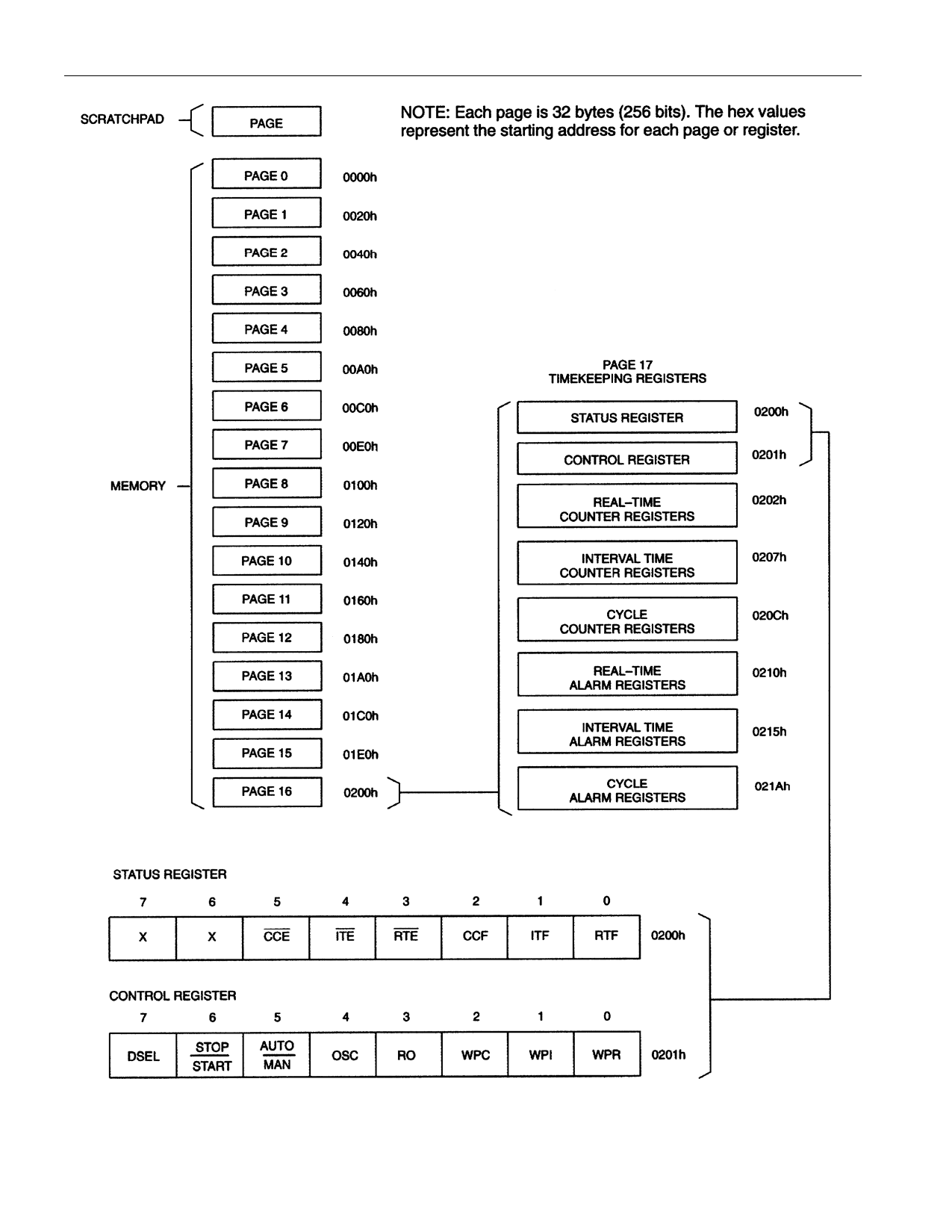
MEMORY MAP Figure 4
DS2404
5 of 29
5 Page 
DS2404
Read Memory [F0h]
The read memory command may be used to read the entire memory. After issuing the command, the user
must provide the 2-byte target address. After the two bytes, the user reads data beginning from the target
address and may continue until the end of memory, at which point logic 1’s will be read. It is important to
realize that the target address registers will contain the address provided. The ending offset/data status
byte is unaffected.
The hardware of the DS2404 provides a means to accomplish error-free writing to the memory section.
To safeguard reading data in the 1-Wire environment and to simultaneously speed up data transfers, it is
recommended to packetize data into data packets of the size of one memory page each. Such a packet
would typically store a 16-bit CRC with each page of data to ensure rapid, error-free data transfers that
eliminate having to read a page multiple times to determine if the received data is correct or not. (See the
Book of DS19xx iButton Standards, Chapter 7 for the recommended file structure to be used with the 1-
Wire environment.)
MEMORY FUNCTION EXAMPLES
Example 1: Write one page of data to page 15
Read page 15 (3-wire port)
MASTER MODE
TX
DATA(LSB FIRST)
Reset
TX 0Fh
TX E0h
TX 01h
TX <32 data bytes>
TX Reset
TX AAh
RX E0h
RX 01h
RX 1Fh
RX <32 data bytes>
TX Reset
TX 55h
TX E0h
TX 01h
TX 1Fh
RX <busy indicator>
TX Reset
TX F0h
TX E0h
TX 01h
RX <32 data bytes>
TX Reset
COMMENTS
Master pulses RST low
Issue “write scratchpad” command
TA1, beginning offset=0
TA2, address=01E0h
Write 1 page of data to scratchpad
Master pulses RST low
Issue “read scratchpad” command
Read TA1, beginning offset=0
Read TA2, address=01E0h
Read E/S, ending offset=31d, flags=0
Read scratchpad data and verify
Master pulses RST low
Issue “copy scratchpad” command
TA1
TA2 AUTHORIZATION CODE
E/S
Wait until DQ=0 (~30 μs typical)
Master pulses RST low
Issue “read memory” command
TA1, beginning offset=0
TA2, address=01E0h
Read memory page 15 and verify
Master pulses RST low, done
NOTE: The ROM function commands do not apply to the 3-wire port. After RST is at a high level, the
device expects to receive a memory function command.
11 of 29
11 Page | ||
| Páginas | Total 29 Páginas | |
| PDF Descargar | [ Datasheet DS2404.PDF ] | |
Hoja de datos destacado
| Número de pieza | Descripción | Fabricantes |
| DS2401 | Silicon Serial Number | Dallas Semiconducotr |
| DS2401 | Silicon Serial Number | Maxim Integrated |
| DS2404 | EconoRAM Time Chip | Dallas Semiconducotr |
| DS2404S-C01 | Dual Port Memory Plus Time | Dallas Semiconducotr |
| Número de pieza | Descripción | Fabricantes |
| SLA6805M | High Voltage 3 phase Motor Driver IC. |
Sanken |
| SDC1742 | 12- and 14-Bit Hybrid Synchro / Resolver-to-Digital Converters. |
Analog Devices |
|
DataSheet.es es una pagina web que funciona como un repositorio de manuales o hoja de datos de muchos de los productos más populares, |
| DataSheet.es | 2020 | Privacy Policy | Contacto | Buscar |
