|
|
|
PDF FM24CL04-S Data sheet ( Hoja de datos )
| Número de pieza | FM24CL04-S | |
| Descripción | 4Kb FRAM Serial Memory | |
| Fabricantes | ETC | |
| Logotipo | ||
Hay una vista previa y un enlace de descarga de FM24CL04-S (archivo pdf) en la parte inferior de esta página. Total 12 Páginas | ||
|
No Preview Available !
FM24CL04
4Kb FRAM Serial Memory
Features
4K bit Ferroelectric Nonvolatile RAM
• Organized as 512 x 8 bits
• Unlimited Read/Writes
• 10 Year Data Retention
• NoDelay™ Writes
• Advanced High-Reliability Ferroelectric Process
Fast Two-wire Serial Interface
• Up to 1 MHz maximum bus frequency
• Direct hardware replacement for EEPROM
Description
The FM24CL04 is a 4-kilobit nonvolatile memory
employing an advanced ferroelectric process. A
ferroelectric random access memory or FRAM is
nonvolatile and performs reads and writes like a
RAM. It provides reliable data retention for 10 years
while eliminating the complexities, overhead, and
system level reliability problems caused by EEPROM
and other nonvolatile memories.
Unlike serial EEPROMs, the FM24CL04 performs
write operations at bus speed. No write delays are
incurred. Data is written to the memory array in the
cycle after it has been successfully transferred to the
device. The next bus cycle may commence
immediately.
These capabilities make the FM24CL04 ideal for
nonvolatile memory applications requiring frequent
or rapid writes. Examples range from data collection
where the number of write cycles may be critical, to
demanding industrial controls where the long write
time of EEPROM can cause data loss. The
combination of features allows more frequent data
writing with less overhead for the system.
The FM24CL04 provides substantial benefits to users
of serial EEPROM, yet these benefits are available in
a hardware drop-in replacement. The FM24CL04 is
available in an industry standard 8-pin package using
a two-wire protocol. The specifications are
guaranteed over an industrial temperature range of -
40°C to +85°C.
Low Power Operation
• 2.7V to 3.65V operation
• 75 µA Active Current (100 kHz) @ 3V
• 1 µA Standby Current
Industry Standard Configuration
• Industrial Temperature -40° C to +85° C
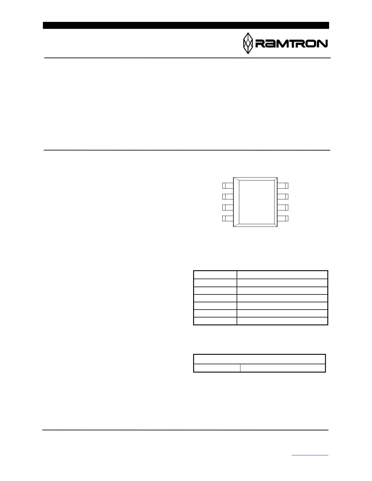
• 8-pin SOIC
Pin Configuration
NC
A1
A2
VSS
1
2
3
4
8 VDD
7 WP
6 SCL
5 SDA
Pin Names
A1-A2
SDA
SCL
WP
VSS
VDD
Function
Device Select Address 1 and 2
Serial Data/Address
Serial Clock
Write Protect
Ground
Supply Voltage 3V
Ordering Information
FM24CL04-S 8-pin SOIC
This product conforms to specifications per the terms of the Ramtron
standard warranty. Production processing does not necessarily in-
clude testing of all parameters.
Rev. 2.0
July 2003
Ramtron International Corporation
1850 Ramtron Drive, Colorado Springs, CO 80921
(800) 545-FRAM, (719) 481-7000, Fax (719) 481-7058
www.ramtron.com
Page 1 of 12
1 page 
Figure 4. Slave Address
No word address occurs for a read operation. Reads
always use the lower 8-bits that are held internally in
the address latch and the 9th address bit is part of the
slave address. Reads always begin at the address
following the previous access. A random read address
can be loaded by doing a write operation as explained
below.
After transmission of each data byte, just prior to the
acknowledge, the FM24CL04 increments the internal
address latch. This allows the next sequential byte to
be accessed with no additional addressing. After the
last address (1FFh) is reached, the address latch will
roll over to 000h. There is no limit to the number of
bytes that can be accessed with a single read or write
operation.
Data Transfer
After all address information has been transmitted,
data transfer between the bus master and the
FM24CL04 can begin. For a read operation the
FM24CL04 will place 8 data bits on the bus then wait
for an acknowledge. If the acknowledge occurs, the
next sequential byte will be transferred. If the
acknowledge is not sent, the read operation is
concluded. For a write operation, the FM24CL04 will
accept 8 data bits from the master then send an
acknowledge. All data transfer occurs MSB (most
significant bit) first.
FM24CL04
Memory Operation
The FM24CL04 is designed to operate in a manner
very similar to other 2-wire interface memory
products. The major differences result from the
higher performance write capability of FRAM
technology. These improvements result in some
differences between the FM24CL04 and a similar
configuration EEPROM during writes. The complete
operation for both writes and reads is explained
below.
Write Operation
All writes begin with a slave address then a word
address. The bus master indicates a write operation
by setting the LSB of the Slave address to a 0. After
addressing, the bus master sends each byte of data to
the memory and the memory generates an
acknowledge condition. Any number of sequential
bytes may be written. If the end of the address range
is reached internally, the address counter will wrap
from 1FFh to 000h.
Unlike other nonvolatile memory technologies, there
is no write delay with FRAM. The entire memory
cycle occurs in less time than a single bus clock.
Therefore any operation including read or write can
occur immediately following a write. Acknowledge
polling, a technique used with EEPROMs to
determine if a write is complete is unnecessary and
will always return a done condition.
An actual memory array write occurs after the 8th
data bit is transferred. It will be complete before the
acknowledge is sent. Therefore if the user desires to
abort a write without altering the memory contents,
this should be done using a start or stop condition
prior to the 8th data bit. The FM24CL04 needs no
page buffering.
Pulling write protect high will disable writes to the
entire array. The FM24CL04 will not acknowledge
data bytes that are written when write protect is
asserted. In addition, the address counter will not
increment if writes are attempted. Pulling WP low
(VSS) will deactivate this feature.
Figure 5 below illustrates both a single- and
multiple- byte write.
Rev. 2.0
July 2003
Page 5 of 12
5 Page 
FM24CL04
Diagram Notes
All start and stop timing parameters apply to both read and write cycles. Clock specifications are identical for read
and write cycles. Write timing parameters apply to slave address, word address, and write data bits. Functional
relationships are illustrated in the relevant data sheet sections. These diagrams illustrate the timing parameters only.
Read Bus Timing
Write Bus Timing
Data Retention (VDD = 2.7V to 3.65V unless otherwise specified)
Parameter
Min Units
Data Retention
10 Years
Notes
1
Notes
1. The relationship between retention, temperature, and the associated reliability
level is characterized separately.
Rev. 2.0
July 2003
Page 11 of 12
11 Page | ||
| Páginas | Total 12 Páginas | |
| PDF Descargar | [ Datasheet FM24CL04-S.PDF ] | |
Hoja de datos destacado
| Número de pieza | Descripción | Fabricantes |
| FM24CL04-S | 4Kb FRAM Serial Memory | ETC |
| Número de pieza | Descripción | Fabricantes |
| SLA6805M | High Voltage 3 phase Motor Driver IC. |
Sanken |
| SDC1742 | 12- and 14-Bit Hybrid Synchro / Resolver-to-Digital Converters. |
Analog Devices |
|
DataSheet.es es una pagina web que funciona como un repositorio de manuales o hoja de datos de muchos de los productos más populares, |
| DataSheet.es | 2020 | Privacy Policy | Contacto | Buscar |