|
|
|
PDF FM24C256EYYX Data sheet ( Hoja de datos )
| Número de pieza | FM24C256EYYX | |
| Descripción | 256 KBit 2-Wire Bus Interface Serial EEPROM with Write Protect | |
| Fabricantes | Fairchild Semiconductor | |
| Logotipo | ||
Hay una vista previa y un enlace de descarga de FM24C256EYYX (archivo pdf) en la parte inferior de esta página. Total 12 Páginas | ||
|
No Preview Available !
June 2000
FM24C256
256 KBit 2-Wire Bus Interface
Serial EEPROM with Write Protect
General Description
The FM24C256/C256L/C256LZ devices are 256 Kbits CMOS
nonvolatile electrically erasable memory. These devices offer the
designer different low voltage and low power options. They
conform to all requirements in the Extended IIC 2-wire protocol.
Furthermore, they are designed to minimize device pin count and
simplify PC board layout requirements.
The entire memory array can be write disabled (Write Protection)
by connecting the WP pin to VCC.
Functional address lines allow up to eight devices on the same
bus, for up to a total of 2 Mbit address space.
The IIC communication protocol uses CLOCK (SCL) and DATA
I/O (SDA) lines to synchronously clock data between the master
(for example a microprocessor) and the slave EEPROM device(s).
Fairchild EEPROMs are designed and tested for applications
requiring high endurance, high reliability, and low power con-
sumption.
Features
I Extended Operating Voltages
— C256: 4.5V - 5.5V
— C256L: 2.7V - 5.5V
— C256LZ: 2.7V - 5.5V
I Low Power CMOS
— 1mA active current typical
— C256/C256L: 10µA standby current typical
— C256LZ: less than 1µA standby current
I 2-wire IIC serial interface
I 64 byte page write mode
I Max write cycle time of 6ms byte/page
I 40 years data retention
I Endurance: 100,000 data changes
I Hardware write protect for entire array
I Schmitt trigger inputs for noise suppression
I Electrostatic discharge protection > 4000V
I 8-pin DIP and 8-pin SO (150 mil) packages. Contact factory
for CSP package availability
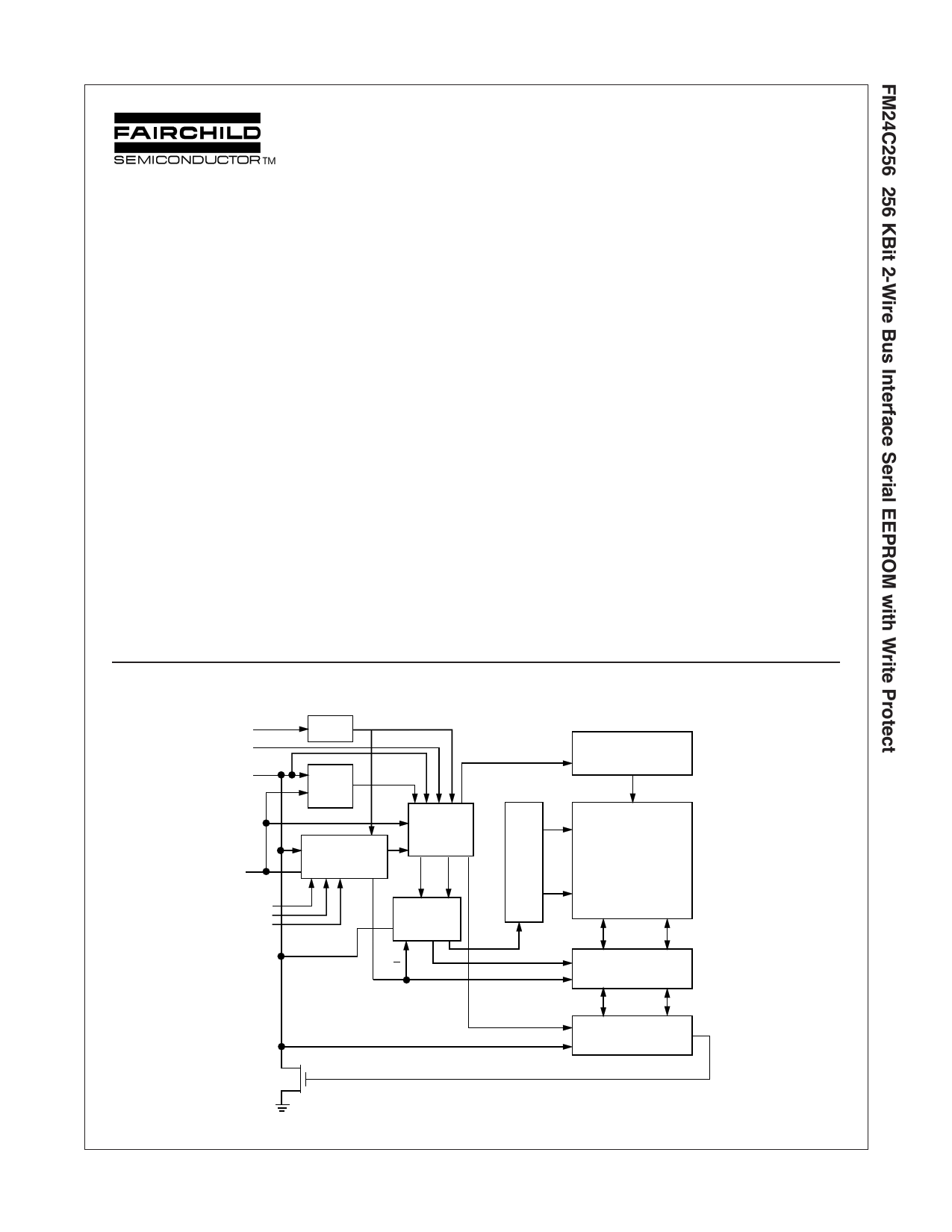
Block Diagram
VCC
WP
SDA
SCL
A2
A1
A0
WRITE
LOCKOUT
START
STOP
LOGIC
START CYCLE
SLAVE ADDRESS
REGISTER &
COMPARATOR
CONTROL
LOGIC
LOAD
INC
WORD
ADDRESS
COUNTER
XDEC
R/W
H.V. GENERATION
TIMING &CONTROL
E2PROM
ARRAY
YDEC
CK
DIN
DATA REGISTER
DOUT
DS800023-1
© 2000 Fairchild Semiconductor International
FM24C256 rev. B.3
1
www.fairchildsemi.com
1 page 
AC Conditions of Test
Input Pulse Levels
Input Rise and Fall Times
VCC x 0.1 to VCC x 0.9
10 ns
Input & Output Timing Levels VCC x 0.5
Output Load
1 TTL Gate and CL = 100 pF
Read and Write Cycle Limits (Standard and Low VCC Range - 2.7V-5.5V)
Symbol
Parameter
100 kHz
Min Max
400 kHz
Min Max
fSCL SCL Clock Frequency
TI Noise Suppression Time Constant at
SCL, SDA Inputs (Minimum VIN
Pulse width)
100
100
400
50
tAA SCL Low to SDA Data Out Valid 0.3 3.5 0.3 1.2
tBUF Time the Bus Must Be Free before
a New Transmission Can Start
4.7
1.3
tHD:STA
tLOW
tHIGH
tSU:STA
Start Condition Hold Time
Clock Low Period
Clock High Period
Start Condition Setup Time
(for a Repeated Start Condition)
4.0
4.7
4.0
4.7
0.6
1.5
0.6
0.6
tHD:DAT
tSU:DAT
tR
tF
tSU:STO
tDH
tWR
(Note 2)
Data in Hold Time
Data in Setup Time
SDA and SCL Rise Time
SDA and SCL Fall Time
Stop Condition Setup Time
Data Out Hold Time
Write Cycle Time
00
250 100
1 0.3
300 300
4.7 0.6
100 100
66
Units
kHz
ns
µs
µs
µs
µs
µs
µs
µs
ns
µs
ns
µs
ns
ms
Note 2: The write cycle time (tWR) is the time from a valid stop condition of a write sequence to the end of the internal erase/program cycle. During the write cycle, the
FM24C256 bus interface circuits are disabled, SDA is allowed to remain high per the bus-level pull-up resistor, and the device does not respond to its slave address
FM24C256 rev. B.3
5 www.fairchildsemi.com
5 Page 
Physical Dimensions inches (millimeters) unless otherwise noted
0.189 - 0.197
(4.800 - 5.004)
87 65
0.228 - 0.244
(5.791 - 6.198)
0.010 - 0.020 x 45¡
(0.254 - 0.508)
0.150 - 0.157
(3.810 - 3.988)
8¡ Max, Typ.
All leads
0.0075 - 0.0098
(0.190 - 0.249)
Typ. All Leads
0.004
(0.102)
All lead tips
0.016 - 0.050
(0.406 - 1.270)
Typ. All Leads
12 34
Lead #1
IDENT
0.053 - 0.069
(1.346 - 1.753)
0.014
(0.356)
0.050
(1.270)
Typ
0.004 - 0.010
(0.102 - 0.254)
Seating
Plane
0.014 - 0.020 Typ.
(0.356 - 0.508)
Molded Small Out-Line Package (M8)
Order Number FM24C256xxxM8 or FM24C256xxxEM8
Package Number M08A
FM24C256 rev. B.3
11 www.fairchildsemi.com
11 Page | ||
| Páginas | Total 12 Páginas | |
| PDF Descargar | [ Datasheet FM24C256EYYX.PDF ] | |
Hoja de datos destacado
| Número de pieza | Descripción | Fabricantes |
| FM24C256EYYX | 256 KBit 2-Wire Bus Interface Serial EEPROM with Write Protect | Fairchild Semiconductor |
| Número de pieza | Descripción | Fabricantes |
| SLA6805M | High Voltage 3 phase Motor Driver IC. |
Sanken |
| SDC1742 | 12- and 14-Bit Hybrid Synchro / Resolver-to-Digital Converters. |
Analog Devices |
|
DataSheet.es es una pagina web que funciona como un repositorio de manuales o hoja de datos de muchos de los productos más populares, |
| DataSheet.es | 2020 | Privacy Policy | Contacto | Buscar |