|
|
|
PDF FGH50N6S2D Data sheet ( Hoja de datos )
| Número de pieza | FGH50N6S2D | |
| Descripción | 600V/ SMPS II Series N-Channel IGBT with Anti-Parallel StealthTM Diode | |
| Fabricantes | Fairchild Semiconductor | |
| Logotipo | ||
Hay una vista previa y un enlace de descarga de FGH50N6S2D (archivo pdf) en la parte inferior de esta página. Total 9 Páginas | ||
|
No Preview Available !
July 2002
FGH50N6S2D
600V, SMPS II Series N-Channel IGBT with Anti-Parallel StealthTM Diode
General Description
The FGH50N6S2D is a Low Gate Charge, Low Plateau
Voltage SMPS II IGBT combining the fast switching speed
of the SMPS IGBTs along with lower gate charge, plateau
voltage and avalanche capability (UIS). These LGC devices
shorten delay times, and reduce the power requirement of
the gate drive. These devices are ideally suited for high volt-
age switched mode power supply applications where low
conduction loss, fast switching times and UIS capability are
essential. SMPS II LGC devices have been specially de-
signed for:
• Power Factor Correction (PFC) circuits
• Full bridge topologies
• Half bridge topologies
• Push-Pull circuits
• Uninterruptible power supplies
• Zero voltage and zero current switching circuits
IGBT (co-pack) formerly Developmental Type TA49344
Diode formerly Developmental Type TA49392
Features
• 100kHz Operation at 390V, 40A
• 200kHZ Operation at 390V, 25A
• 600V Switching SOA Capability
• Typical Fall Time. . . . . . . . . . . 90ns at TJ = 125oC
• Low Gate Charge . . . . . . . . . 70nC at VGE = 15V
• Low Plateau Voltage . . . . . . . . . . . . .6.5V Typical
• UIS Rated . . . . . . . . . . . . . . . . . . . . . . . . . 480mJ
• Low Conduction Loss
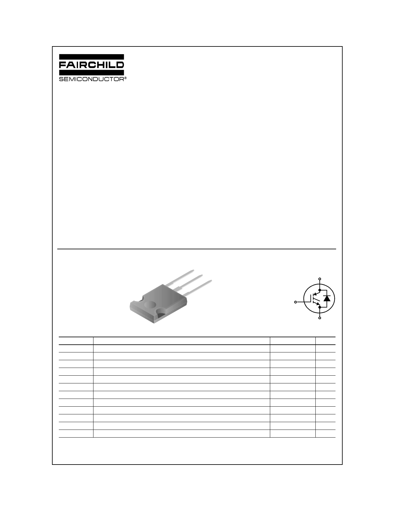
Package
JEDEC STYLE TO-247
E
C
G
Symbol
C
G
E
Device Maximum Ratings TC= 25°C unless otherwise noted
Symbol
Parameter
Ratings
Units
BVCES Collector to Emitter Breakdown Voltage
600 V
IC25 Collector Current Continuous, TC = 25°C
75 A
IC110
Collector Current Continuous, TC = 110°C
60 A
ICM Collector Current Pulsed (Note 1)
240 A
VGES
Gate to Emitter Voltage Continuous
±20 V
VGEM Gate to Emitter Voltage Pulsed
±30 V
SSOA Switching Safe Operating Area at TJ = 150°C, Figure 2
150A at 600V
EAS Pulsed Avalanche Energy, ICE = 30A, L = 1mH, VDD = 50V
480 mJ
PD Power Dissipation Total TC = 25°C
463 W
Power Dissipation Derating TC > 25°C
3.7 W/°C
TJ Operating Junction Temperature Range
-55 to 150
°C
TSTG
Storage Junction Temperature Range
-55 to 150
°C
CAUTION: Stresses above those listed in “Absolute Maximum Ratings” may cause permanent damage to the device. This is a stress only rating and
operation of the device at these or any other conditions above those indicated in the operational sections of this specification is not implied.
NOTE:
1. Pulse width limited by maximum junction temperature.
©2002 Fairchild Semiconductor Corporation
FGH50N6S2D RevA2
1 page 
Typical Performance Curves TJ = 25°C unless otherwise noted
250
225
DUTY CYCLE < 0.5%, VCE = 10V
PULSE DURATION = 250µs
200
175
150
125
100
TJ = 125oC
75
TJ = 25oC
50
TJ = -55oC
25
0
456789
VGE, GATE TO EMITTER VOLTAGE (V)
Figure 13. Transfer Characteristic
10
16
IG(REF) = 1mA, RL = 10Ω
14
12
VCE = 600V
10
VCE = 400V
8
6
4
VCE = 200V
2
0
0 10 20 30 40 50 60 70 80
QG, GATE CHARGE (nC)
Figure 14. Gate Charge
3.0
RG = 3Ω, L = 200µH, VCE = 390V, VGE = 15V
ETOTAL = EON2 + EOFF
2.5
ICE = 60A
2.0
1.5
ICE = 30A
1.0
ICE = 15A
0.5
100
TJ = 125oC, L = 200µH, VCE = 390V, VGE = 15V
ETOTAL = EON2 + EOFF
10
ICE = 60A
ICE = 30A
1
ICE = 15A
0
25
50 75 100 125
TC, CASE TEMPERATURE (oC)
150
Figure 15. Total Switching Loss vs Case
Temperature
4.0
FREQUENCY = 1MHz
3.5
3.0
1
2.5
CIES
2.0
1.5
1.0
0.5
0.0
0
COES
CRES
10 20 30 40 50 60 70 80 90 100
VCE, COLLECTOR TO EMITTER VOLTAGE (V)
Figure 17. Capacitance vs Collector to Emitter
Voltage
0.1
1.0
10 100
RG, GATE RESISTANCE (Ω)
1000
Figure 16. Total Switching Loss vs Gate
Resistance
2.5
DUTY CYCLE < 0.5%
PULSE DURATION = 250µs
2.4
2.3
ICE = 45A
2.2
2.1
ICE = 30A
2.0
1.9
ICE = 15A
1.8
1.7
6 7 8 9 10 11 12 13 14 15 16
VGE, GATE TO EMITTER VOLTAGE (V)
Figure 18. Collector to Emitter On-State Voltage vs
Gate to Emitter Voltage
©2002 Fairchild Semiconductor Corporation
FGH50N6S2D RevA2
5 Page | ||
| Páginas | Total 9 Páginas | |
| PDF Descargar | [ Datasheet FGH50N6S2D.PDF ] | |
Hoja de datos destacado
| Número de pieza | Descripción | Fabricantes |
| FGH50N6S2 | 600V/ SMPS II Series N-Channel IGBT | Fairchild Semiconductor |
| FGH50N6S2D | 600V/ SMPS II Series N-Channel IGBT with Anti-Parallel StealthTM Diode | Fairchild Semiconductor |
| Número de pieza | Descripción | Fabricantes |
| SLA6805M | High Voltage 3 phase Motor Driver IC. |
Sanken |
| SDC1742 | 12- and 14-Bit Hybrid Synchro / Resolver-to-Digital Converters. |
Analog Devices |
|
DataSheet.es es una pagina web que funciona como un repositorio de manuales o hoja de datos de muchos de los productos más populares, |
| DataSheet.es | 2020 | Privacy Policy | Contacto | Buscar |